Datasheet 搜索 > 光耦合器/光隔离器 > Fairchild(飞兆/仙童) > H11G1SM 数据手册 > H11G1SM 其他数据使用手册 4/65 页
 器件3D模型
¥ 2.055
H11G1SM 其他数据使用手册 - Fairchild(飞兆/仙童)
制造商:
Fairchild(飞兆/仙童)
分类:
光耦合器/光隔离器
封装:
PDIP-6
描述:
Fairchild Semiconductor### 光耦合器,Fairchild Semiconductor
Pictures:
3D模型
符号图
焊盘图
引脚图
产品图
页面导航:
导航目录
H11G1SM数据手册
Page:
of 65 Go
若手册格式错乱,请下载阅览PDF原文件

SM320C6201B, SMJ320C6201B
DIGITAL SIGNAL PROCESSOR
SGUS031B -- APRIL 2000 -- REVISED AUGUST 2001
4
POST OFFICE BOX 1443 HOUSTON, TEXAS 77251--1443
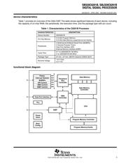
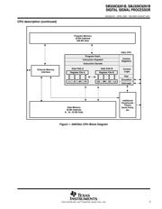
CPU description
The CPU fetches Ve lociTI advanced very-long instruction words (VLIW) (256 bits wide) to supply up to eight
32-bit instructions to the eight functional units during every clock cycle. The VelociTI VLIW architecture features
controls by which all eight units do not have to be supplied with instructions if they are not ready to execute. The
first bit of every 32-bit instruction determines if the next instruction belongs to the same execute packet as the
previous instruction, or whether it should be executed in the following clock as a part of the next execute packet.
Fetch packets are always 256 bits wide; however, the execute packets can vary in size. The variable-length
execute packets are a key memory-saving feature, distinguishing the C62x CPU from other VLIW architectures.
The CPU features two sets of functional units. Each s et contains four units and a register file. One set contains
functional units .L1, .S1, .M1, and .D1; the other set contains units .D2, .M2, .S2, and .L2. The two register files
each contain 16 32-bit registers for a total of 32 general-purpose registers. The two sets of functional units, along
with two register files, compose sides A and B of the CPU (see Figure 1 and Figure 2). The four functional units
on each side of the CPU can freely share the 16 registers belonging to that side. Additionally, each side features
a single data bus connected to all the registers on the other side, by which the two sets of functional units can
access data from the register files on the opposite side. While register access by functional units on the same
side of the CPU as the register file can service all the units in a single clock cycle, register access using the
register file across the CPU supports one read and one write per cycle.
Another key feature of the C62x CPU is the load/store architecture, where all instructions operate on registers
(as opposed to data in memory). Two sets of data-addressing units (.D1 and .D2) are responsible for all data
transfers between the register files and the memory. The data address driven by the .D units allows data
addresses generated from one register file to be used to load or store data to or from the other register file. The
C62x CPU supports a variety of indirect addressing modes using either linear- or circular-addressing modes
with 5- or 15-bit offsets. All instructions are conditional, and most can access any one of the 32 registers. Some
registers, however, are singled out to support specific addressing or to hold the condition for conditional
instructions (if the condition is not automatically “true”). The two .M functional units are dedicated for multiplies.
The two .S and .L functional units perform a general set of arithmetic, logical, and branch functions with results
available every clock cycle.
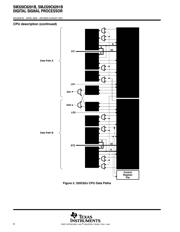
The processing flow begins when a 256-bit-wide instruction fetch packet is fetched from a program memory.
The 32-bit instructions destined for the individual functional units are “ linked” together by “1” bits in the least
significant bit (LSB) position of the instructions. The instructions that are “chained” together for simultaneous
execution (up to eight in total) compose an execute packet. A “0” in the LSB of an instruction breaks the chain,
effectively placing the instructions that follow it in the next execute packet. If an execute packet crosses the fetch
packet boundary (256 bits wide), the assembler places it in the next fetch packet, while the remainder of the
current fetch packet is padded with NOP instructions. The number of execute packets within a fetch packet can
vary from one to eight. Execute packets are dispatched to their respective functional units at the rate of one per
clock cycle and the next 256-bit fetch packet is not fetched until all the execute packets from the current fetch
packet have been dispatched. After decoding, the instructions simultaneously drive all active functional units
for a maximum execution rate of eight instructions every clock cycle. While most results are stored in 32-bit
registers, they can be subsequently moved to memory as bytes or half-words as well. All load and store
instructions are byte-, half-word, or word-addressable.
器件 Datasheet 文档搜索
AiEMA 数据库涵盖高达 72,405,303 个元件的数据手册,每天更新 5,000 多个 PDF 文件
