Datasheet 搜索 > RF模块、IC及配件 > ADI(亚德诺) > HMC361S8GETR 数据手册 > HMC361S8GETR 其他数据使用手册 1/6 页
 器件3D模型
¥ 1.079
HMC361S8GETR 其他数据使用手册 - ADI(亚德诺)
制造商:
ADI(亚德诺)
分类:
RF模块、IC及配件
封装:
SOIC-8
Pictures:
3D模型
符号图
焊盘图
引脚图
产品图
页面导航:
原理图在P3
应用领域在P3
导航目录
HMC361S8GETR数据手册
Page:
of 6 Go
若手册格式错乱,请下载阅览PDF原文件
AN-1463
APPLICATION NOTE
One Technology Way • P. O. Box 9106 • Norwood, MA 02062-9106, U.S.A. • Tel: 781.329.4700 • Fax: 781.461.3113 • www.analog.com
Frequency Divider Operation and Compensation with No Input Signal
Rev. A | Page 1 of 6
INTRODUCTION
The Analog Devices, Inc., prescalar product line includes
more than 10 low noise, static dividers utilizing indium gallium
phosphide (InGaP) and gallium arsenide (GaAs) heterojunction
bipolar transistor (HBT) technology that accept a broad range
of input signals, from dc (with a square wave input) through
18 GHz microwave frequencies. Division ratios of 2, 3, 4, 5, and
8 are available together with 3 V and 5 V single-supply versions.
These divider products exhibit very low additive single-sideband
(SSB) phase noise with the best products delivering −153 dBc/Hz
at 100 kHz offset, enabling synthesizer designers to maintain
excellent system noise performance. This application note
describes how to prevent self oscillation and subsequent false
triggers in the dividers when no radio frequency (RF) power is
presented at the device input.
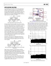
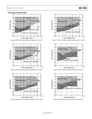
APPLICATION PROBLEM
Dividers are used in a wide variety of applications ranging from
consumer electronics to military and satellite systems. Specifically,
dividers are incorporated in circuits such as phase-locked loops
(PLLs) or synthesizers. In each of these applications, the RF
signal is continuously incident on the input of the frequency
divider, presenting it with a constant dominant signal (signal-
to-noise ratio (SNR) high). However, other applications may
not present a continuous RF signal to the input, thereby leaving
the input vulnerable to noise (SNR low). One such application
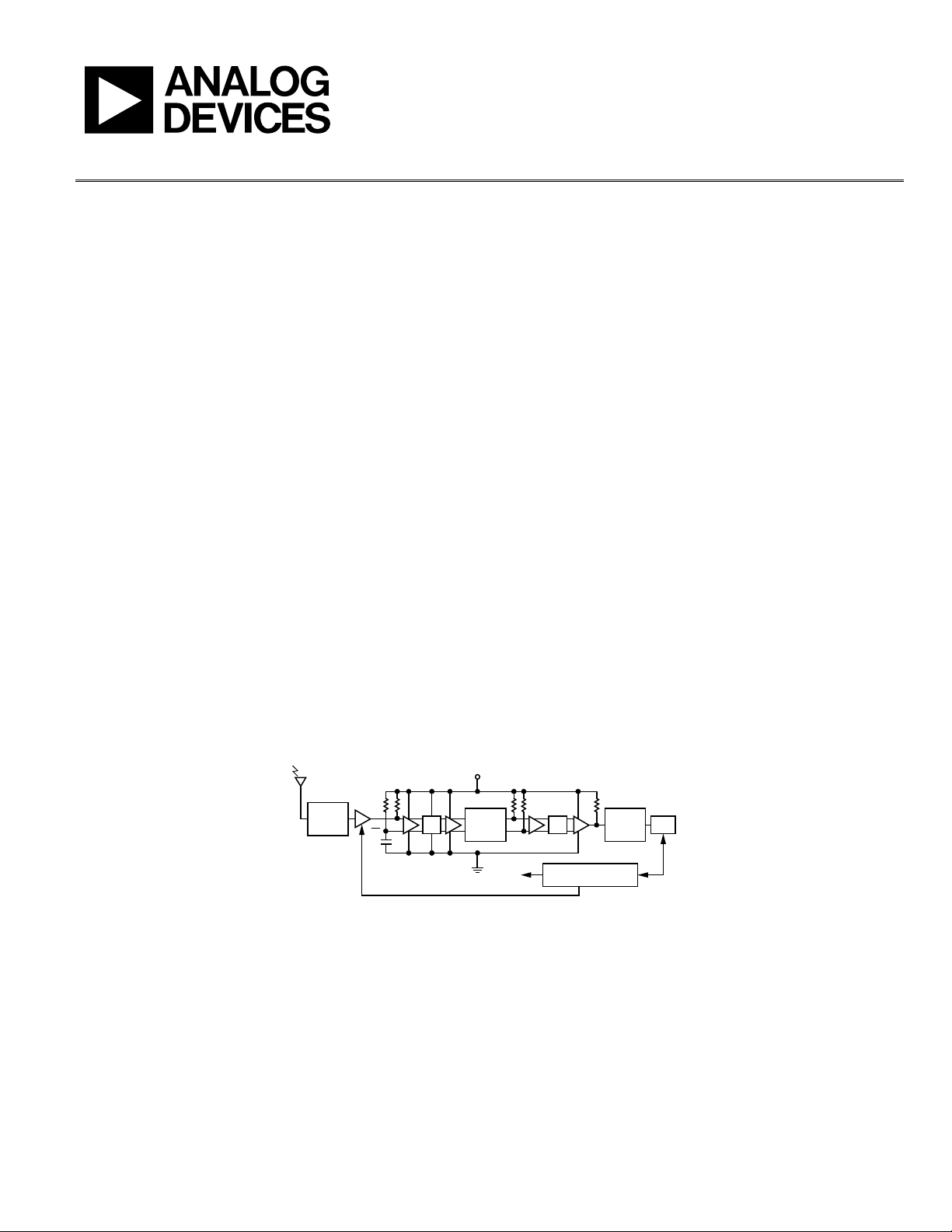
is a signal detection circuit, shown in Figure 1. This circuit
detects the presence of RF energy by directly downconverting
through multiple divider circuits and performing an analog-to-
digital transformation. The signal detection circuitry determines
the frequency and then outputs the appropriate response.
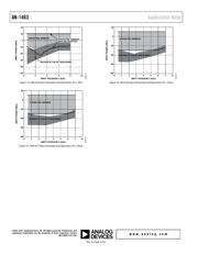
When no input is present, the inputs to the dividers are subjected
to noise. Because the dividers are designed for maximum
sensitivity, the input stages have a tendency to self oscillate with
no or low signal input levels. This self oscillation tendency also
causes the dividers to malfunction when the input signal slew
rate is too low, such as with low frequency sine waves. Because
the divider network is essentially digital in nature, any signal
with a sufficient level triggers a gate within the divider; the divider
produces an output due to this false trigger. This output appears
as multiple tones when viewed on a spectrum analyzer. The
tones are detected by the signal detection circuitry, causing a
false output to occur. Therefore, it is essential to prevent the
divider from false triggering in the absence of an RF signal. To
prevent this condition, an offset voltage is applied across the
inputs of the dividers to prevent the self oscillation and, therefore,
the false triggering of the divider in the absence of a signal.
BAND-
PASS
FILTER
LOW-
PASS
FILTER
LOW-
PASS
FILTER
÷ ÷
VCC
SIGNAL DETECTION
CIRCUITRY
DETECT
OUT
ADC
15808-001
AUTOMATIC
GAIN
CONTROL
IN
Figure 1. Signal Detection Circuit
器件 Datasheet 文档搜索
AiEMA 数据库涵盖高达 72,405,303 个元件的数据手册,每天更新 5,000 多个 PDF 文件
