Datasheet 搜索 > MOS管 > Infineon(英飞凌) > IRL2703STRL 数据手册 > IRL2703STRL 其他数据使用手册 2/10 页

¥ 0
IRL2703STRL 其他数据使用手册 - Infineon(英飞凌)
制造商:
Infineon(英飞凌)
分类:
MOS管
封装:
TO-263-3
Pictures:
3D模型
符号图
焊盘图
引脚图
产品图
页面导航:
封装尺寸在P8
标记信息在P8
技术参数、封装参数在P1
电气规格在P2
导航目录
IRL2703STRL数据手册
Page:
of 10 Go
若手册格式错乱,请下载阅览PDF原文件
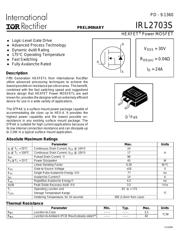
IRL2703S
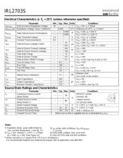
Parameter Min. Typ. Max. Units Conditions
V
(BR)DSS
Drain-to-Source Breakdown Voltage 30 ––– ––– V V
GS
= 0V, I
D
= 250µA
∆V
(BR)DSS
/∆T
J
Breakdown Voltage Temp. Coefficient ––– 0.030 ––– V/°C Reference to 25°C, I
D
= 1mA
––– ––– 0.040 V
GS
= 10V, I
D
= 14A
––– ––– 0.060 V
GS
= 4.5V, I
D
= 12A
V
GS(th)
Gate Threshold Voltage 1.0 ––– ––– V V
DS
= V
GS
, I
D
= 250µA
g
fs
Forward Transconductance 6.4 ––– ––– S V
DS
= 25V, I
D
= 14A
––– ––– 25 V
DS
= 30V, V
GS
= 0V
––– ––– 250 V
DS
= 24V, V
GS
= 0V, T
J
= 150°C
Gate-to-Source Forward Leakage ––– ––– 100 V
GS
= 16V
Gate-to-Source Reverse Leakage ––– ––– -100 V
GS
= -16V
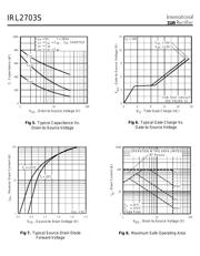
Q
g
Total Gate Charge ––– ––– 15 I
D
= 14A
Q
gs
Gate-to-Source Charge ––– ––– 4.6 nC V
DS
= 24V
Q
gd
Gate-to-Drain ("Miller") Charge ––– ––– 9.3 V
GS
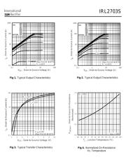
= 4.5V, See Fig. 6 and 13
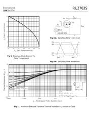
t
d(on)
Turn-On Delay Time ––– 8.5 ––– V
DD
= 15V
t
r
Rise Time ––– 140 ––– I
D
= 14A
t
d(off)
Turn-Off Delay Time ––– 12 ––– R
G
= 12Ω, V
GS
= 4.5V
t
f
Fall Time ––– 20 ––– R
D
= 1.0Ω, See Fig. 10
Between lead,
and center of die contact
C
iss
Input Capacitance ––– 450 ––– V
GS
= 0V
C
oss
Output Capacitance ––– 210 ––– pF V
DS
= 25V
C
rss
Reverse Transfer Capacitance ––– 110 ––– ƒ = 1.0MHz, See Fig. 5
Electrical Characteristics @ T
J
= 25°C (unless otherwise specified)
nA
I
DSS
Drain-to-Source Leakage Current
R
DS(on)
Static Drain-to-Source On-Resistance
I
GSS
ns
µA
Ω
nH
L
S
Internal Source Inductance ––– 7.5 –––
Source-Drain Ratings and Characteristics
Repetitive rating; pulse width limited by
max. junction temperature. ( See fig. 11 )
I
SD
≤ 14A, di/dt ≤ 140A/µs, V
DD
≤ V
(BR)DSS
,
T
J
≤ 175°C
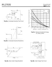
Notes:
V
DD
= 15V, starting T
J
= 25°C, L = 570µH
R
G
= 25Ω, I
AS
= 14A. (See Figure 12)
Pulse width ≤ 300µs; duty cycle ≤ 2%.
** When mounted on 1" square PCB ( FR-4 or G-10 Material ).
For recommended footprint and soldering techniques refer to application note #AN-994.
Uses IRL2703 data and test conditions.
Parameter Min. Typ. Max. Units Conditions
I
S
Continuous Source Current MOSFET symbol
(Body Diode) showing the
I
SM
Pulsed Source Current integral reverse
(Body Diode) p-n junction diode.
V
SD
Diode Forward Voltage ––– ––– 1.3 V T
J
= 25°C, I
S
= 14A, V
GS
= 0V
t
rr
Reverse Recovery Time ––– 65 97 ns T
J
= 25°C, I
F
= 14A
Q
rr
Reverse RecoveryCharge ––– 140 210 nC di/dt = 100A/µs
t
on
Forward Turn-On Time Intrinsic turn-on time is negligible (turn-on is dominated by L
S
+L
D
)
A
––– ––– 96
––– ––– 24
S
D
G
器件 Datasheet 文档搜索
AiEMA 数据库涵盖高达 72,405,303 个元件的数据手册,每天更新 5,000 多个 PDF 文件
