Datasheet 搜索 > 运算放大器 > TI(德州仪器) > LMC6482IMX/NOPB 数据手册 > LMC6482IMX/NOPB 其他数据使用手册 2/35 页
 器件3D模型
¥ 6.436
LMC6482IMX/NOPB 其他数据使用手册 - TI(德州仪器)
制造商:
TI(德州仪器)
分类:
运算放大器
封装:
SOIC-8
描述:
TEXAS INSTRUMENTS LMC6482IMX/NOPB 芯片, 运算放大器, 1.5MHz, 1.3V/uS, SOIC-8
Pictures:
3D模型
符号图
焊盘图
引脚图
产品图
页面导航:
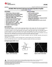
典型应用电路图在P20P21
封装尺寸在P28P30P31
标记信息在P28P29
封装信息在P28P29P30P31
技术参数、封装参数在P2
应用领域在P1P17P22P24P35
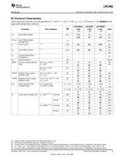
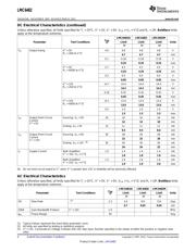
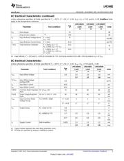
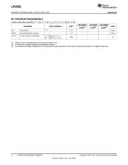
电气规格在P2P3P4P5P6P7P8P9P10P11P12P13
导航目录
LMC6482IMX/NOPB数据手册
Page:
of 35 Go
若手册格式错乱,请下载阅览PDF原文件
LMC6482
SNOS674D –NOVEMBER 1997–REVISED MARCH 2013
www.ti.com
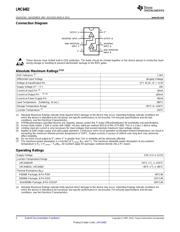
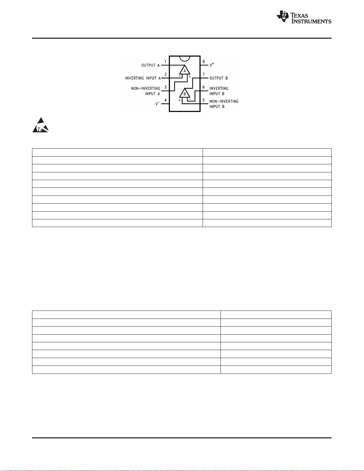
Connection Diagram
These devices have limited built-in ESD protection. The leads should be shorted together or the device placed in conductive foam
during storage or handling to prevent electrostatic damage to the MOS gates.
Absolute Maximum Ratings
(1)(2)
ESD Tolerance
(3)
1.5kV
Differential Input Voltage ±Supply Voltage
Voltage at Input/Output Pin (V
+
) +0.3V, (V
−
) −0.3V
Supply Voltage (V
+
− V
−
) 16V
Current at Input Pin
(4)
±5mA
Current at Output Pin
(5) (6)
±30mA
Current at Power Supply Pin 40mA
Lead Temperature (Soldering, 10 sec.) 260°C
Storage Temperature Range −65°C to +150°C
Junction Temperature
(7)
150°C
(1) Absolute Maximum Ratings indicate limits beyond which damage to the device may occur. Operating Ratings indicate conditions for
which the device is intended to be functional, but specific performance is not ensured. For ensured specifications and the test
conditions, see the Electrical Characteristics.
(2) If Military/Aerospace specified devices are required, please contact the TI Sales Office/Distributors for availability and specifications.
(3) Human body model, 1.5kΩ in series with 100pF. All pins rated per method 3015.6 of MIL-STD-883. This is a Class 1 device rating.
(4) Limiting input pin current is only necessary for input voltages that exceed absolute maximum input voltage ratings.
(5) Applies to both single-supply and split-supply operation. Continuous short circuit operation at elevated ambient temperature can result in
exceeding the maximum allowed junction temperature of 150°C. Output currents in excess of ±30mA over long term may adversely
affect reliability.
(6) Do not short circuit output to V
+
, when V
+
is greater than 13V or reliability will be adversely affected.
(7) The maximum power dissipation is a function of T
J(max)
, θ
JA
, and T
A
. The maximum allowable power dissipation at any ambient
temperature is P
D
= (T
J(max)
− T
A
)/θ
JA
. All numbers apply for packages soldered directly into a PC board.
Operating Ratings
Supply Voltage 3.0V ≤ V+ ≤ 15.5V
Junction Temperature Range
LMC6482AM −55°C ≤ T
J
≤ +125°C
LMC6482AI, LMC6482I −40°C ≤ T
J
≤ +85°C
Thermal Resistance (θ
JA
)
P0008E Package, 8-Pin PDIP 90°C/W
D0008A Package, 8-Pin SOIC 155°C/W
DGK0008A Package, 8-Pin VSSOP 194°C/W
(1) Absolute Maximum Ratings indicate limits beyond which damage to the device may occur. Operating Ratings indicate conditions for
which the device is intended to be functional, but specific performance is not ensured. For ensured specifications and the test
conditions, see the Electrical Characteristics.
2 Submit Documentation Feedback Copyright © 1997–2013, Texas Instruments Incorporated
Product Folder Links: LMC6482
器件 Datasheet 文档搜索
AiEMA 数据库涵盖高达 72,405,303 个元件的数据手册,每天更新 5,000 多个 PDF 文件
