Datasheet 搜索 > 比较器 > TI(德州仪器) > LMC7221BIMX 数据手册 > LMC7221BIMX 其他数据使用手册 4/13 页

 器件3D模型
¥ 14.193
LMC7221BIMX 其他数据使用手册 - TI(德州仪器)
制造商:
TI(德州仪器)
分类:
比较器
封装:
SOIC-8
描述:
LMC7221微型CMOS比较器,轨至轨输入和开漏输出 LMC7221 Tiny CMOS Comparator with Rail-To-Rail Input and Open Drain Output
Pictures:
3D模型
符号图
焊盘图
引脚图
产品图
页面导航:
导航目录
LMC7221BIMX数据手册
Page:
of 13 Go
若手册格式错乱,请下载阅览PDF原文件
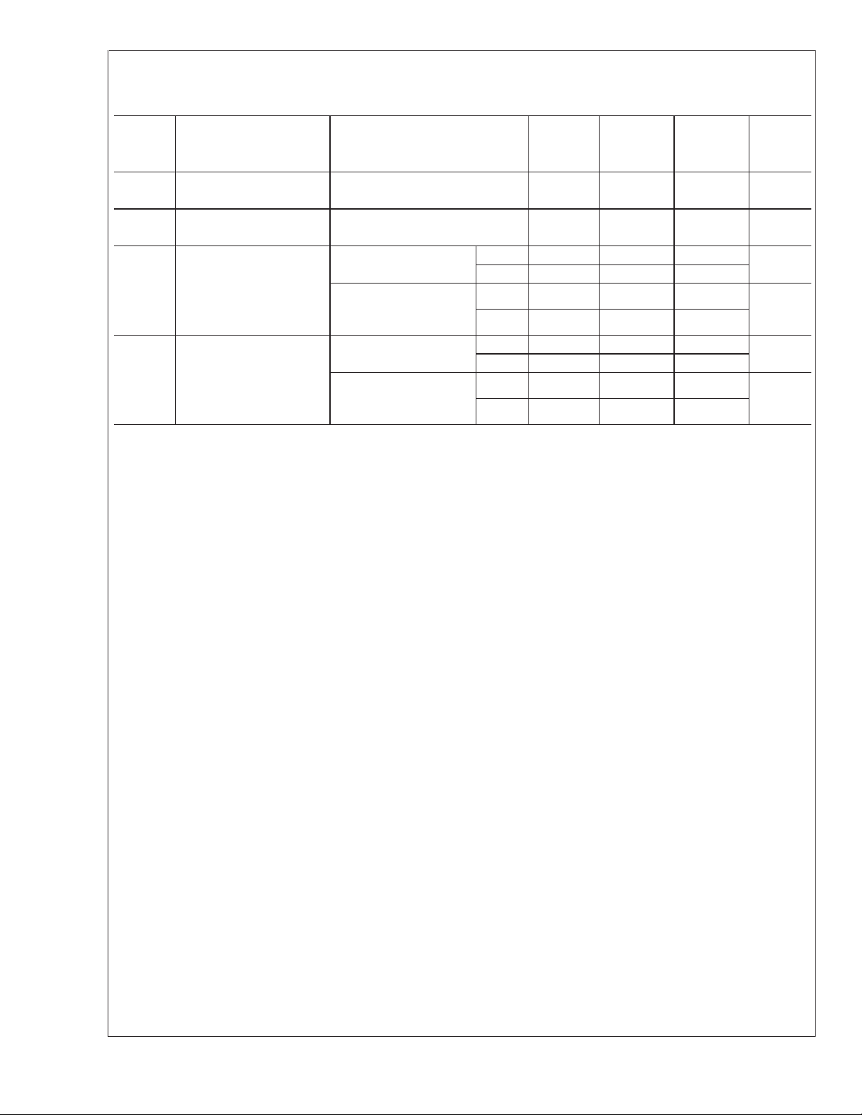
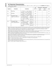
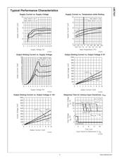
AC Electrical Characteristics
Unless otherwise specified, all limits guaranteed for T
J
= 25˚C, V
+
= 5V, V
−
= 0V, V
CM
=V
O
=V
+
/2. Boldface limits apply at
the temperature extreme.
Typ LMC7221AI LMC7221BI
Symbol Parameter Conditions (Note 5) Limit Limit Units
(Note 6) (Note 6)
t
rise
Rise Time f = 10 kHz, C
L
= 50 pF, (Note 8) 0.3 µs
Overdrive = 10 mV, 5 kΩ Pullup
t
fall
Fall Time f = 10 kHz, C
L
= 50 pF, (Note 8) 0.3 µs
Overdrive = 10 mV, 5 kΩ Pullup
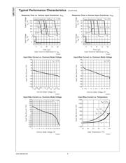
t
PHL
Propagation Delay
(High to Low) (Note 10)
f = 10 kHz, C
L
=50pF,
5kΩ Pullup (Note 8)
10 mV 10
µs
100 mV 4
V
+
= 2.7V,f=10kHz,
C
L
=50pF,5kΩ Pullup
(Note 8)
10 mV 10
µs
100 mV 4
t
PLH
Propagation Delay
(Low to High) (Note 10)
f = 10 kHz, C
L
=50pF,
5kΩ Pullup (Note 8)
10 mV 6
µs
100 mV 4
V
+
= 2.7V,f=10kHz,
C
L
=50pF,5kΩ Pullup
(Note 8)
10 mV 7
µs
100 mV 4
Note 1: Absolute Maximum Ratings indicate limits beyond which damage to the device may occur. Operating Ratings indicate conditions for which the device is
intended to be functional, but specific performance is not guaranteed. For guaranteed specifications and the test conditions, see the Electrical Characteristics.
Note 2: Human Body Model, applicable std. MIL-STD-883, Method 3015.7. Machine Model, applicable std. JESD22-A115-A (ESD MM std. of JEDEC)
Field-Induced Charge-Device Model, applicable std. JESD22-C101-C (ESD FICDM std. of JEDEC).
Note 3: Applies to both single-supply and split-supply operation. Continuous short circuit operation at elevated ambient temperature can result in exceeding the
maximum allowed junction temperature of 150˚C. Output currents in excess of
±
30 mA may adversely affect reliability.
Note 4: The maximum power dissipation is a function of T
J(MAX)
, θ
JA
. The maximum allowable power dissipation at any ambient temperature is P
D
=(T
J(MAX)
–T
A
)/
θ
JA
. All numbers apply for packages soldered directly onto a PC Board.
Note 5: Typical values represent the most likely parametric norm as determined at the time of characterization. Actual typical values may vary over time and will
also depend on the application and configuration. The typical values are not tested and are not guaranteed on shipped production material.
Note 6: All limits are guaranteed by testing or statistical analysis.
Note 7: Limiting input pin current is only necessary for input voltages which exceed the absolute maximum input voltage rating.
Note 8: Do not short circuit the output to V
+
when V
+
is greater than 12V or reliability will be adversely affected.
Note 9: C
L
includes the probe and test jig capacitance.
Note 10: Input offset voltage average drift is calculated by dividing the accelerated operating life V
OS
drift by the equivalent operational time. This represents worst
case input conditions and includes the first 30 days of drift.
Note 11: Input step voltage for propagation delay measurement is 2V.
LMC7221
www.national.com 4
器件 Datasheet 文档搜索
AiEMA 数据库涵盖高达 72,405,303 个元件的数据手册,每天更新 5,000 多个 PDF 文件
