Datasheet 搜索 > 比较器 > TI(德州仪器) > LMC7225IMX 数据手册 > LMC7225IMX 产品封装文件 3/11 页

 器件3D模型
¥ 6.255
LMC7225IMX 产品封装文件 - TI(德州仪器)
制造商:
TI(德州仪器)
分类:
比较器
封装:
SOIC-8
Pictures:
3D模型
符号图
焊盘图
引脚图
产品图
页面导航:
导航目录
LMC7225IMX数据手册
Page:
of 11 Go
若手册格式错乱,请下载阅览PDF原文件
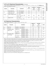
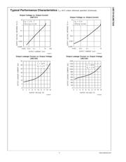
2.7V to 5V Electrical Characteristics (Continued)
Unless otherwise specified, all limits guaranteed for T
J
= 25˚C, V
+
= 2.7V to 5V, V
−
= 0V, V
CM
=V
O
=V
+
/2. Boldface limits
apply at the temperature extremes.
Typ LMC7215 LMC7225
Symbol Parameter Conditions (Note 5) Limit Limit Units
(Note 6) (Note 6)
Current (Note 10) V
+
= 5.0V, Sourcing 50 NA mA
I
SC−
Output Short Circuit V
+
= 2.7V, Sinking 12 mA
Current (Note 10) V
+
= 5.0V, Sinking 30 mA
I
Leakage
Output Leakage Current V
+
= 2.2V nA
V
IN
+ = 0.1V, V
IN
− = 0V, 0.01 NA 500 max
V
OUT
= 15V
I
S
Supply Current V
+
= 5.0V 0.7 1 1 µA
V
IN
+ = 5V, V
IN
−=0V 1.2 1.2 max
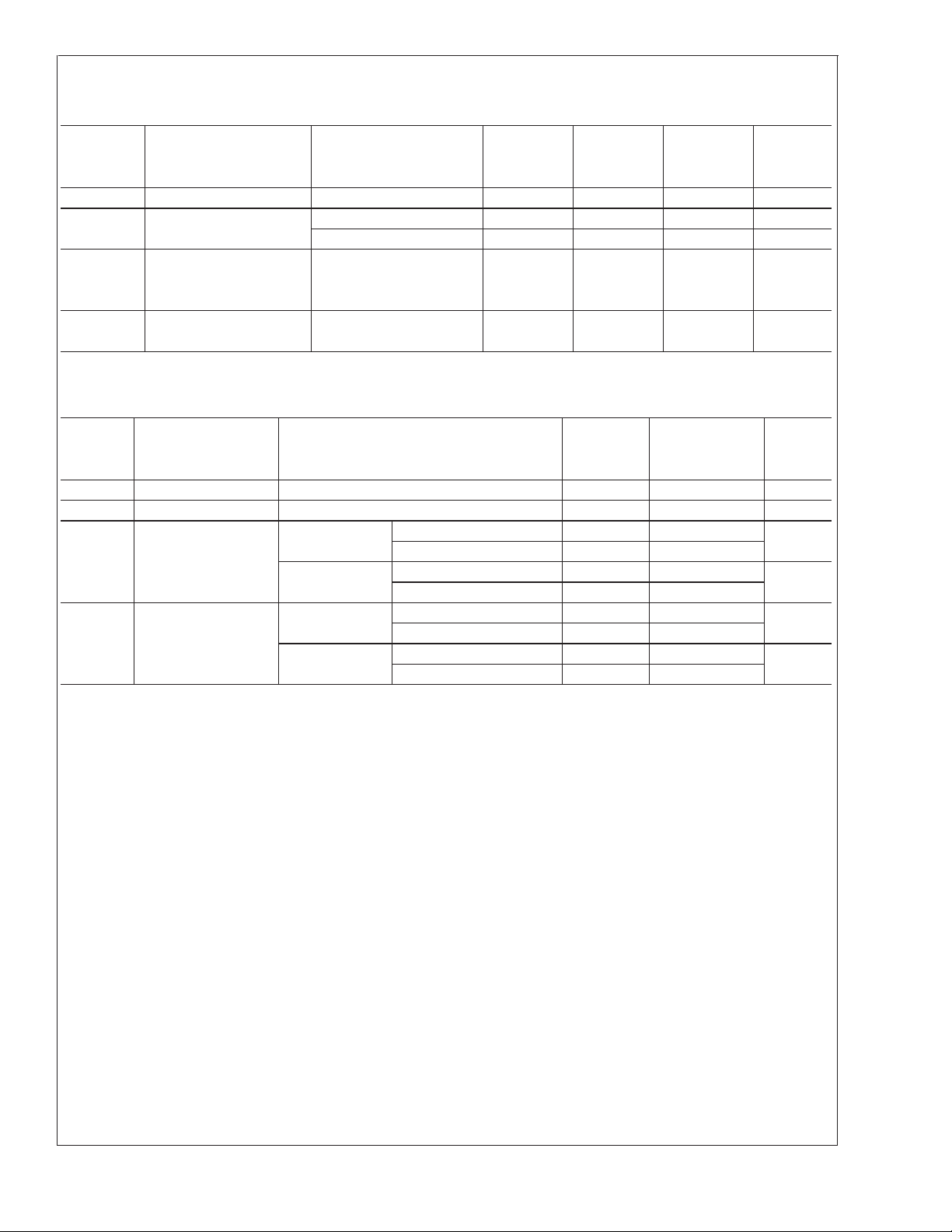
AC Electrical Characteristics
Unless otherwise specified, T
J
= 25˚C, V
+
= 5V, V
−
= 0V, V
CM
=V
+
/2
LMC7215 LMC7225
Symbol Parameter Conditions Typ Typ Units
(Note 5) (Notes 5, 8)
t
rise
Rise Time Overdrive = 10 mV (Note 8) 1 12.2 µs
t
fall
Fall Time Overdrive = 10 mV (Note 8) 0.4 0.35 µs
t
PHL
Propagation Delay (Notes 8, 9) Overdrive = 10 mV 24 24 µs
(High to Low) Overdrive = 100 mV 12 12
V
+
= 2.7V Overdrive = 10 mV 17 17 µs
(Notes 8, 9) Overdrive = 100 mV 11 11
t
PLH
Propagation Delay (Notes 8, 9) Overdrive = 10 mV 24 29 µs
(Low to High) Overdrive = 100 mV 12 17
V
+
= 2.7V Overdrive = 10 mV 17 22 µs
(Notes 8, 9) Overdrive = 100 mV 11 16
Note 1: Absolute Maximum Ratings indicate limits beyond which damage to the device may occur. Operating Ratings indicate conditions for which the device is
intended to be functional, but specific performance is not guaranteed. For guaranteed specifications and the test conditions, see the Electrical Characteristics.
Note 2: Human Body Model, applicable std. MIL-STD-883, Method 3015.7. Machine Model, applicable std. JESD22-A115-A (ESD MM std. of JEDEC)
Field-Induced Charge-Device Model, applicable std. JESD22-C101-C (ESD FICDM std. of JEDEC).
Note 3: Applies to both single-supply and split-supply operation. Continuous short circuit operation at elevated ambient temperature can result in exceeding the
maximum allowed junction temperature of 150˚C.
Note 4: The maximum power dissipation is a function of T
J(MAX)
, θ
JA
, and T
A
. The maximum allowable power dissipation at any ambient temperature is
P
D
=(T
J(MAX)
−T
A
)/θ
JA
. All numbers apply for packages soldered directly into a PC board.
Note 5: Typical values represent the most likely parametric norm as determined at the time of characterization. Actual typical values may vary over time and will
also depend on the application and configuration. The typical values are not tested and are not guaranteed on shipped production material.
Note 6: All limits are guaranteed by testing or statistical analysis.
Note 7: CMRR measured at V
CM
= 0V to 2.5V and 2.5V to 5V when V
S
=5V,V
CM
= 0.2V to 1.35V and 1.35V to 2.7V when V
S
= 2.7V. This eliminates units that
have large V
OS
at the V
CM
extremes and low or opposite V
OS
at V
CM
=V
S
/2.
Note 8: All measurements made at 10 kHz. A 100 kΩ pull-up resistor was used when measuring the LMC7225. C
LOAD
= 50 pF including the test jig and scope
probe. The rise times of the LMC7225 are a function of the R-C time constant.
Note 9: Input step voltage for the propagation measurements is 100 mV.
Note 10: Do not short the output of the LMC7225 to voltages greater than 10V or damage may occur.
LMC7215/LMC7225
www.national.com3
器件 Datasheet 文档搜索
AiEMA 数据库涵盖高达 72,405,303 个元件的数据手册,每天更新 5,000 多个 PDF 文件
