Datasheet 搜索 > 微控制器 > NXP(恩智浦) > LPC2292FBD144/01,5 数据手册 > LPC2292FBD144/01,5 其他数据使用手册 1/54 页
 器件3D模型
¥ 98.592
LPC2292FBD144/01,5 其他数据使用手册 - NXP(恩智浦)
制造商:
NXP(恩智浦)
分类:
微控制器
封装:
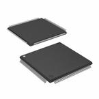
LQFP-144
描述:
ARM7 系列微控制器,NXP一系列 NXP 微控制器,基于 16/32 位 ARM7TDMI-S CPU ,带实时仿真和嵌入式追踪支持,将微控制器与 32 kB、64 kB、128 kB、256 kB 和 512 KB 嵌入式高速闪存相结合。 128 位宽存储器接口和独特的加速器体系结构实现在最大时钟频率时使用 32 位代码。高集成和低功耗 一系列串行通信接口和片上 SRAM 选项 备选 16 位 Thumb 模式将代码缩小 30%,而性能削弱最少。 32 位计时器,PWM 通道和多达 47 条 GPIO 线路 适用于工业控制和医疗系统 ### ARM7/9 微控制器,NXP
Pictures:
3D模型
符号图
焊盘图
引脚图
产品图
页面导航:

导航目录
LPC2292FBD144/01,5数据手册
Page:
of 54 Go
若手册格式错乱,请下载阅览PDF原文件

1. General description
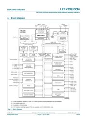
The LPC2292/2294 microcontrollers are based on a 16/32-bit ARM7TDMI-S CPU with
real-time emulation and embedded trace support, together with 256 kB of embedded
high-speed flash memory. A 128-bit wide memory interface and a unique accelerator
architecture enable 32-bit code execution at the maximum clock rate. For critical code
size applications, the alternative 16-bit Thumb mode reduces code by more than 30 %
with minimal performance penalty.
With their 144-pin package, low power consumption, various 32-bit timers, 8-channel
10-bit ADC, 2/4 (LPC2294) advanced CAN channels, PWM channels and up to nine
external interrupt pins these microcontrollers are particularly suitable for automotive and
industrial control applications as well as medical systems and fault-tolerant maintenance
buses. The number of available GPIOs ranges from 76 (with external memory) through
112 (single-chip). With a wide range of additional serial communications interfaces, they
are also suited for communication gateways and protocol converters as well as many
other general-purpose applications.
Remark: Throughout the data sheet, the term LPC2292/2294 will apply to devices with
and without the /00 or /01 suffix. The suffixes /00 and /01 will be used to differentiate from
other devices only when necessary.
2. Features and benefits
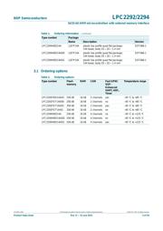
2.1 Key features brought by LPC2292/2294/01 devices
Fast GPIO ports enable port pin toggling up to 3.5 times faster than the original device.
They also allow for a port pin to be read at any time regardless of its function.
Dedicated result registers for ADC(s) reduce interrupt overhead. The ADC pads are
5 V tolerant when configured for digital I/O function(s).
UART0/1 include fractional baud rate generator, auto-bauding capabilities and
handshake flow-control fully implemented in hardware.
Buffered SSP serial controller supporting SPI, 4-wire SSI, and Microwire formats.
SPI programmable data length and master mode enhancement.
Diversified Code Read Protection (CRP) enables different security levels to be
implemented. This feature is available in LPC2292/2294/00 devices as well.
General purpose timers can operate as external event counters.
2.2 Key features common for all devices
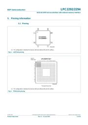
16/32-bit ARM7TDMI-S microcontroller in a LQFP144 package.
LPC2292/2294
16/32-bit ARM microcontrollers; 256 kB ISP/IAP flash with
CAN, 10-bit ADC and external memory interface
Rev. 8 — 8 June 2011 Product data sheet
器件 Datasheet 文档搜索
AiEMA 数据库涵盖高达 72,405,303 个元件的数据手册,每天更新 5,000 多个 PDF 文件
