Datasheet 搜索 > 微控制器 > NXP(恩智浦) > LPC2292FBD144/01,5 数据手册 > LPC2292FBD144/01,5 其他数据使用手册 2/54 页
 器件3D模型
¥ 13.658
LPC2292FBD144/01,5 其他数据使用手册 - NXP(恩智浦)
制造商:
NXP(恩智浦)
分类:
微控制器
封装:
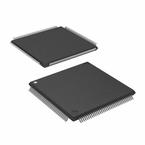
LQFP-144
描述:
ARM7 系列微控制器,NXP一系列 NXP 微控制器,基于 16/32 位 ARM7TDMI-S CPU ,带实时仿真和嵌入式追踪支持,将微控制器与 32 kB、64 kB、128 kB、256 kB 和 512 KB 嵌入式高速闪存相结合。 128 位宽存储器接口和独特的加速器体系结构实现在最大时钟频率时使用 32 位代码。高集成和低功耗 一系列串行通信接口和片上 SRAM 选项 备选 16 位 Thumb 模式将代码缩小 30%,而性能削弱最少。 32 位计时器,PWM 通道和多达 47 条 GPIO 线路 适用于工业控制和医疗系统 ### ARM7/9 微控制器,NXP
Pictures:
3D模型
符号图
焊盘图
引脚图
产品图
页面导航:

导航目录
LPC2292FBD144/01,5数据手册
Page:
of 54 Go
若手册格式错乱,请下载阅览PDF原文件

LPC2292_2294 All information provided in this document is subject to legal disclaimers. © NXP B.V. 2011. All rights reserved.
Product data sheet Rev. 8 — 8 June 2011 2 of 54
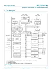
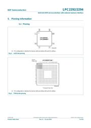
NXP Semiconductors
LPC2292/2294
16/32-bit ARM microcontrollers with external memory interface
16 kB on-chip static RAM and 256 kB on-chip flash program memory. 128-bit wide
interface/accelerator enables high-speed 60 MHz operation.
In-System Programming/In-Application Programming (ISP/IAP) via on-chip bootloader
software. Single flash sector or full chip erase in 400 ms and programming of 256 B in
1 ms.
EmbeddedICE-RT and Embedded Trace interfaces offer real-time debugging with the
on-chip RealMonitor software as well as high-speed real-time tracing of instruction
execution.
Two/four (LPC2292/2294) interconnected CAN interfaces with advanced acceptance
filters. Additional serial interfaces include two UARTs (16C550), Fast I
2
C-bus
(400 kbit/s) and two SPIs.
Eight channel 10-bit ADC with conversion time as low as 2.44 s.
Two 32-bit timers (with four capture and four compare channels), PWM unit (six
outputs), Real-Time Clock (RTC), and watchdog.
Vectored Interrupt Controller (VIC) with configurable priorities and vector addresses.
Configurable external memory interface with up to four banks, each up to 16 MB and
8/16/32-bit data width.
Up to 112 general purpose I/O pins (5 V tolerant). Up to nine edge/level sensitive
external interrupt pins available.
60 MHz maximum CPU clock available from programmable on-chip PLL with settling
time of 100 s.
The on-chip crystal oscillator should have an operating range of 1 MHz to 25 MHz.
Power saving modes include Idle and Power-down.
Processor wake-up from Power-down mode via external interrupt.
Individual enable/disable of peripheral functions for power optimization.
Dual power supply:
CPU operating voltage range of 1.65 V to 1.95 V (1.8 V 0.15 V).
I/O power supply range of 3.0 V to 3.6 V (3.3 V 10 %) with 5 V tolerant I/O pads.
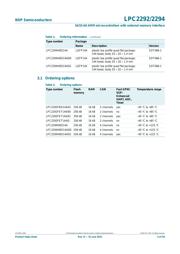
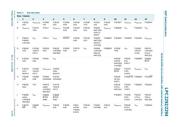
3. Ordering information
Table 1. Ordering information
Type number Package
Name Description Version
LPC2292FBD144/01 LQFP144 plastic low profile quad flat package;
144 leads; body 20 20 1.4 mm
SOT486-1
LPC2292FET144/00 TFBGA144 plastic thin fine-pitch ball grid array package;
144 balls; body 12 12 0.8 mm
SOT569-2
LPC2292FET144/01 TFBGA144 plastic thin fine-pitch ball grid array package;
144 balls; body 12 12 0.8 mm
SOT569-2
LPC2292FET144/G TFBGA144 plastic thin fine-pitch ball grid array package;
144 balls; body 12 12 0.8 mm
SOT569-2
器件 Datasheet 文档搜索
AiEMA 数据库涵盖高达 72,405,303 个元件的数据手册,每天更新 5,000 多个 PDF 文件
