Datasheet 搜索 > 稳压芯片 > ON Semiconductor(安森美) > NCP1117DTAG 数据手册 > NCP1117DTAG 其他数据使用手册 4/19 页

¥ 4.317
NCP1117DTAG 其他数据使用手册 - ON Semiconductor(安森美)
制造商:
ON Semiconductor(安森美)
分类:
稳压芯片
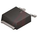
封装:
TO-252-3
描述:
ON SEMICONDUCTOR NCP1117DTAG 新
Pictures:
3D模型
符号图
焊盘图
引脚图
产品图
页面导航:
引脚图在P1Hot
典型应用电路图在P2
封装尺寸在P17P18
焊盘布局在P18
型号编码规则在P1P12P13P19
标记信息在P1P14P15P16P17P18P19
封装信息在P12P13
技术参数、封装参数在P12P13
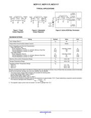
应用领域在P1P2P9P13
电气规格在P3P4
型号编号列表在P2
导航目录
NCP1117DTAG数据手册
Page:
of 19 Go
若手册格式错乱,请下载阅览PDF原文件
NCP1117, NCP1117I, NCV1117
www.onsemi.com
4
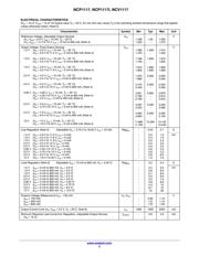
ELECTRICAL CHARACTERISTICS (continued)
(C
in
= 10 mF, C
out
= 10 mF, for typical value T
A
= 25°C, for min and max values T
A
is the operating ambient temperature range that applies
unless otherwise noted.) (Note 4)
Characteristic UnitMaxTypMinSymbol
Quiescent Current
1.5 V (V
in
= 11.5 V)
1.8 V (V
in
= 11.8 V)
1.9 V (V
in
= 11.9 V)
2.0 V (V
in
= 12 V)
2.5 V (V
in
= 10 V)
2.85 V (V
in
= 10 V)
3.3 V (V
in
= 15 V)
5.0 V (V
in
= 15 V)
12 V (V
in
= 20 V)
I
Q
−
−
−
−
−
−
−
−
−
3.6
4.2
4.3
4.5
5.2
5.5
6.0
6.0
6.0
10
10
10
10
10
10
10
10
10
mA
Thermal Regulation (T
A
= 25°C, 30 ms Pulse) − 0.01 0.1 %/W
Ripple Rejection (V
in
−V
out
= 6.4 V, I
out
= 500 mA, 10 V
pp
120 Hz Sinewave)
Adjustable
1.5 V
1.8 V
1.9 V
2.0 V
2.5 V
2.85 V
3.3 V
5.0 V
12 V
RR
67
66
66
66
64
62
62
60
57
50
73
72
70
72
70
68
68
64
61
54
−
−
−
−
−
−
−
−
−
−
dB
Adjustment Pin Current (V
in
= 11.25 V, I
out
= 800 mA) I
adj
− 52 120
mA
Adjust Pin Current Change
(V
in
−V
out
= 1.4 V to 10 V, I
out
= 10 mA to 800 mA)
DI
adj
− 0.4 5.0
mA
Temperature Stability S
T
− 0.5 − %
Long Term Stability (T
A
= 25°C, 1000 Hrs End Point Measurement) S
t
− 0.3 − %
RMS Output Noise (f = 10 Hz to 10 kHz) N − 0.003 − %V
out
Product parametric performance is indicated in the Electrical Characteristics for the listed test conditions, unless otherwise noted. Product
performance may not be indicated by the Electrical Characteristics if operated under different conditions.
4. NCP1117: T
low
= 0°C, T
high
= 125°C
NCP1117I: T
low
= −40°C, T
high
= 125°C
NCV1117: T
low
= −40°C, T
high
= 125°C
5. Low duty cycle pulse techniques are used during testing to maintain the junction temperature as close to ambient as possible.
6. The regulator output current must not exceed 1.0 A with V
in
greater than 12 V.
器件 Datasheet 文档搜索
AiEMA 数据库涵盖高达 72,405,303 个元件的数据手册,每天更新 5,000 多个 PDF 文件
