Datasheet 搜索 > 微控制器 > Microchip(微芯) > PIC16C74A-20I/PQ 数据手册 > PIC16C74A-20I/PQ 其他数据使用手册 2/8 页

 器件3D模型
¥ 114.072
PIC16C74A-20I/PQ 其他数据使用手册 - Microchip(微芯)
制造商:
Microchip(微芯)
分类:
微控制器
封装:
QFP-44
描述:
8位CMOS微控制器与A / D转换器 8-Bit CMOS Microcontrollers with A/D Converter
Pictures:
3D模型
符号图
焊盘图
引脚图
产品图
页面导航:
技术参数、封装参数在P5
导航目录
PIC16C74A-20I/PQ数据手册
Page:
of 8 Go
若手册格式错乱,请下载阅览PDF原文件
PIC16C74A
DS80089A-page 2 2001 Microchip Technology Inc.
3. Module: CCP (Compare Mode)
The special event trigger of the Compare mode
may not occur if both of the following conditions
exist:
• An instruction, one cycle (T
CY) prior to a
Timer1/Compare register match has literal
data equal to the address of a CCP register
being used. Specific cases include:
• An instruction in the same cycle as a
Timer1/Compare register match has an
MSb of ‘0’.
The interrupt for the compare event will still be
generated, but no special event trigger will occur.
Work around
Use the Interrupt Service Routine instead of using
the special event trigger to reset Timer1 (and start
an A/D conversion, if applicable).
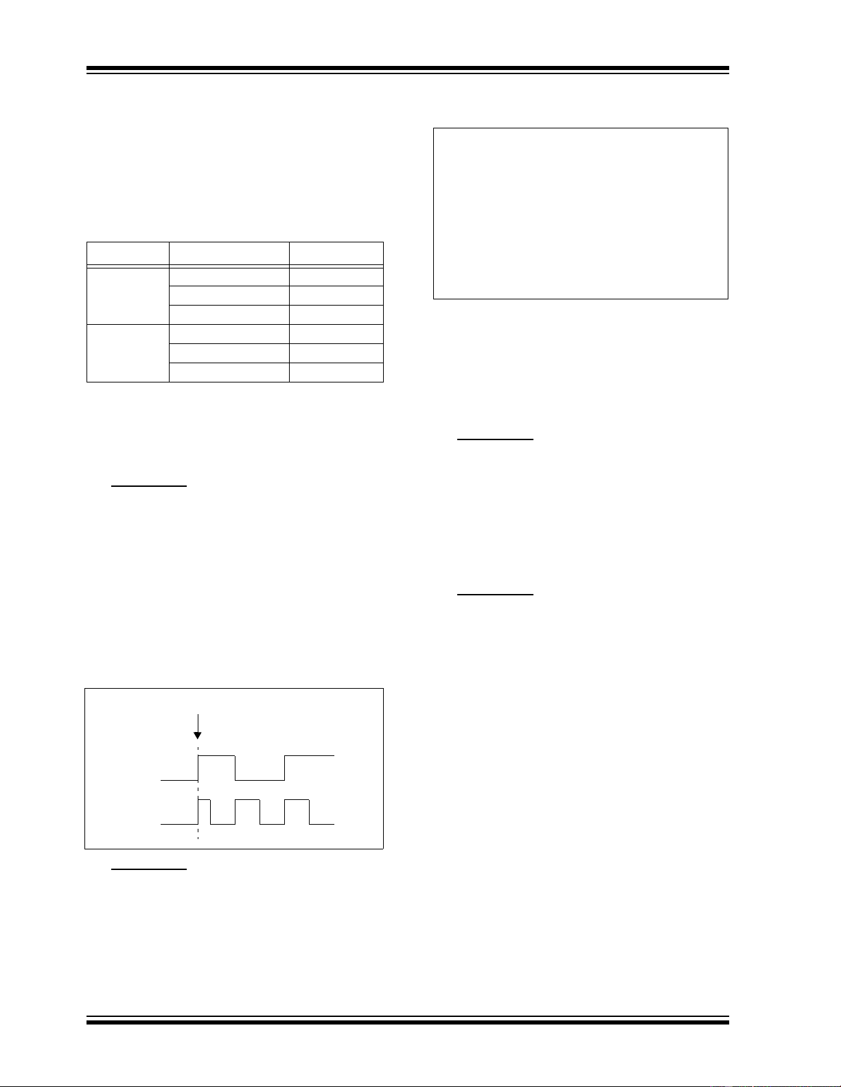
4. Module: SSP (SPI Mode)
When the SPI is using Timer2/2 as the clock
source, a shorter than expected SCK pulse may
occur on the first bit of the transmitted/received
data (Figure 1).
FIGURE 1: SCK PULSE VARIATION
USING TIMER2/2
Work around
To avoid producing the short pulse, turn off Timer2
and clear the TMR2 register, load the SSPBUF
with the data to transmit, and then turn Timer2
back on. Refer to Example 1 for sample code.
EXAMPLE 1: AVOIDING THE INITIAL
SHORT SCK PULSE
5. Module: SSP Module (I
2
C™ mode)
If the bus is active when the I
2
C mode is enabled,
and the next 8 bits of data on the bus match the
address of the device, then the SSP module will
generate an Acknowledge pulse.
Work around
Before enabling the I
2
C mode, ensure that the bus
is not active.
6. Module: Timer0
The TMR0 register may increment when the WDT
postscaler is switched to the Timer0 prescaler. If
TMR0 = FFh, this will cause TMR0 to overflow
(setting T0IF).
Work around
Follow the following sequence:
a) Read the 8-bit TMR0 register into the
W register
b) Clear the TMR0 register
c) Assign WDT postscaler to Timer0
d) Write W register to TMR0
Unit Register Literal Data
CCP1
CCPR1L 15h
CCPR1H 16h
CCP1CON 17h
CCP2
CCPR2L 1Bh
CCPR2H 1Ch
CCP2C0N 1Dh
SD0
SCK
Write SSPBUF
bit0=1 bit1=0 bit2=1
. . . .
BSF STATUS, RP0 ;Bank 1
LOOP BTFSS SSPSTAT,BF ;Data received?
;(Xmit complete?)
GOTO LOOP ;No
BCF STATUS, RP0 ;Bank 0
MOVF SSPBUF, W ;W = SSPBUF
MOVWF RXDATA ;Save in user RAM
MOVF TXDATA, W ;W = TXDATA
BCF T2CON, TMR2ON ;Timer2 off
CLR TMR2 ;Clear Timer2
MOVWF SSPBUF ;Xmit New data
BSF T2CON, TMR2ON ;Timer2 on
器件 Datasheet 文档搜索
AiEMA 数据库涵盖高达 72,405,303 个元件的数据手册,每天更新 5,000 多个 PDF 文件
