Datasheet 搜索 > Microchip(微芯) > PIC18F47K42-I/ML 数据手册 > PIC18F47K42-I/ML 其他数据使用手册 2/803 页
 器件3D模型
¥ 5.824
PIC18F47K42-I/ML 其他数据使用手册 - Microchip(微芯)
制造商:
Microchip(微芯)
封装:
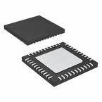
QFN-44
Pictures:
3D模型
符号图
焊盘图
引脚图
产品图
页面导航:
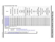
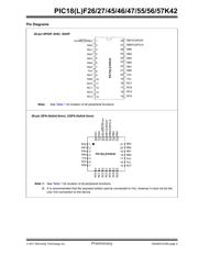
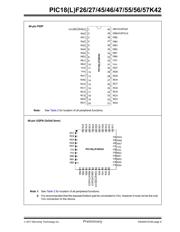
引脚图在P5P23P283P343P353P473P658P659Hot
典型应用电路图在P596P659
原理图在P26P79P91P100P109P177P227P229P230P273P284P296
封装尺寸在P771
标记信息在P767P768P769P770
封装信息在P767P772P773P774P776P780P781P782P784P785P786P787
功能描述在P226
技术参数、封装参数在P93P173P174P178P204P644P645P745P751P752P754P755
应用领域在P77P654
电气规格在P173P174P178P204P645
导航目录
PIC18F47K42-I/ML数据手册
Page:
of 803 Go
若手册格式错乱,请下载阅览PDF原文件

2017 Microchip Technology Inc. Preliminary DS40001919A-page 2
PIC18(L)F26/27/45/46/47/55/56/57K42
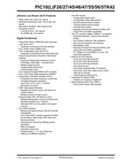
eXtreme Low-Power (XLP) Features
• Sleep mode: 60 nA @ 1.8V, typical
• Windowed Watchdog Timer: 720 nA @ 1.8V,
typical
• Secondary Oscillator: 580 nA @ 32 kHz
• Operating Current:
- 4 uA @ 32 kHz, 1.8V, typical
- 45 uA/MHz @ 1.8V, typical
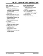
Digital Peripherals
• Three 8-Bit Timers (TMR2/4/6) with Hardware
Limit Timer (HLT)
- Hardware monitoring and Fault detection
• Four 16-Bit Timers (TMR0/1/3/5)
• Four Configurable Logic Cell (CLC):
- Integrated combinational and sequential logic
• Three Complementary Waveform Generators
(CWGs):
- Rising and falling edge dead-band control
- Full-bridge, half-bridge, 1-channel drive
- Multiple signal sources
- Programmable dead band
- Fault-shutdown input
• Four Capture/Compare/PWM (CCP) modules
• Four 10-bit Pulse-Width Modulators (PWMs)
• Numerically Controlled Oscillator (NCO):
- Generates true linear frequency control and
increased frequency resolution
- Input Clock: 0 Hz < f
NCO < 32 MHz
- Resolution: f
NCO/220
• DSM: Data Signal Modulator
- Multiplex two carrier clocks, with glitch pre-
vention feature
- Multiple sources for each carrier
• Programmable CRC with Memory Scan:
- Reliable data/program memory monitoring for
fail-safe operation (e.g., Class B)
- Calculate CRC over any portion of program
memory
• Two UART Modules:
- Modules are Asynchronous, RS-232, RS-485
compatibility.
- One of the UART modules supports LIN Mas-
ter and Slave, DMX mode, DALI Gear and
Device protocols
- Automatic and user-timed BREAK period
generation
- DMA Compatible
- Automatic checksums
- Programmable 1, 1.5, and 2 Stop bits
- Wake-up on BREAK reception
• One SPI module:
- Configurable length bytes
- Configurable length data packets
- Receive-without-transmit option
- Transmit-without-receive option
- Transfer byte counter
- Separate Transmit and Receive Buffers with
2-byte FIFO and DMA capabilities
•Two I
2
C modules, SMBus, PMBus™ compatible:
- Dedicated Address, Transmit and Receive
buffers
- Bus Collision Detection with arbitration
- Bus time-out detection and handling
- Multi-Master mode
- Separate Transmit and Receive Buffers with
2-byte FIFO and DMA capabilities
-I
2
C, SMBus 2.0 and SMBus 3.0, and 1.8V
input level selections
• Device I/O Port Features:
- 25 I/O pins (PIC18(L)F2xK42)
- 36 I/O pins (PIC18(L)F4xK42)
- 44 I/O pins (PIC18(L)F5xK42)
- One input-only pin
- Individually programmable I/O direction,
open-drain, slew rate, weak pull-up control
- Interrupt-on-change
- Three External Interrupt Pins
• Peripheral Pin Select (PPS):
- Enables pin mapping of digital I/O
• Signal Measurement Timer (SMT):
- 24-bit timer/counter with prescaler
器件 Datasheet 文档搜索
AiEMA 数据库涵盖高达 72,405,303 个元件的数据手册,每天更新 5,000 多个 PDF 文件
