Datasheet 搜索 > MOS管 > ST Microelectronics(意法半导体) > STD7N52K3 数据手册 > STD7N52K3 产品封装文件 5/22 页

¥ 5.075
STD7N52K3 产品封装文件 - ST Microelectronics(意法半导体)
制造商:
ST Microelectronics(意法半导体)
分类:
MOS管
封装:
TO-252-3
描述:
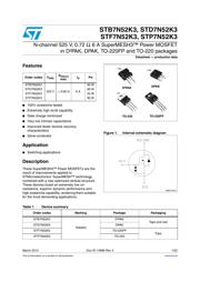
N 通道 MDmesh™ K3 系列,SuperMESH3™, STMicroelectronics### MOSFET 晶体管,STMicroelectronics
Pictures:
3D模型
符号图
焊盘图
引脚图
产品图
页面导航:
导航目录
STD7N52K3数据手册
Page:
of 22 Go
若手册格式错乱,请下载阅览PDF原文件
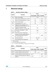
STB7N52K3, STD7N52K3, STF7N52K3, STP7N52K3 Electrical characteristics
Doc ID 14896 Rev 4 5/22
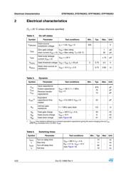
Table 7. Source drain diode
Symbol Parameter Test conditions Min. Typ. Max. Unit
I
SD
I
SDM
(1)
1. Pulse width limited by safe operating area
Source-drain current
Source-drain current (pulsed)
-
6
24
A
A
V
SD
(2)
2. Pulsed: Pulse duration = 300 µs, duty cycle 1.5%
Forward on voltage I
SD
= 6 A, V
GS
= 0 - 1.5 V
t
rr
Q
rr
I
RRM
Reverse recovery time
Reverse recovery charge
Reverse recovery current
I
SD
= 6 A, di/dt = 100 A/µs
V
DD
= 60 V (see Figure 24)
-
220
1800
16
ns
nC
A
t
rr
Q
rr
I
RRM
Reverse recovery time
Reverse recovery charge
Reverse recovery current
I
SD
= 6 A, di/dt = 100 A/µs
V
DD
= 60 V, T
j
= 150 °C
(see Figure 24)
-
250
2200
18
ns
nC
A
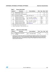
Table 8. Gate-source Zener diode
Symbol Parameter Test conditions Min. Typ. Max. Unit
BV
GSO
(1)
1. The built-in back-to-back Zener diodes have specifically been designed to enhance not only the device’s
ESD capability, but also to make them safely absorb possible voltage transients that may occasionally be
applied from gate to source. In this respect the Zener voltage is appropriate to achieve an efficient and
cost-effective intervention to protect the device’s integrity. These integrated Zener diodes thus avoid the
usage of external components
Gate-source breakdown
voltage
Igs=± 1 mA (open drain) 30 - V
器件 Datasheet 文档搜索
AiEMA 数据库涵盖高达 72,405,303 个元件的数据手册,每天更新 5,000 多个 PDF 文件
