Datasheet 搜索 > 微控制器 > ST Microelectronics(意法半导体) > STM32F103R6T6 数据手册 > STM32F103R6T6 其他数据使用手册 6/83 页
 器件3D模型
¥ 31.863
STM32F103R6T6 其他数据使用手册 - ST Microelectronics(意法半导体)
制造商:
ST Microelectronics(意法半导体)
分类:
微控制器
封装:
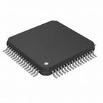
LQFP-64
描述:
性能线,基于ARM的32位MCU和Flash , USB , CAN , 7个16位定时器,2个ADC和9通信接口 Performance line, ARM-based 32-bit MCU with Flash, USB, CAN, seven 16-bit timers, two ADCs and nine communication interfaces
Pictures:
3D模型
符号图
焊盘图
引脚图
产品图
页面导航:
引脚图在P18P19P20P21P22P23P24P25P26P63Hot
典型应用电路图在P46P66
封装尺寸在P68
型号编码规则在P76P77P78
封装信息在P68P69P70P71P72P73P74P75P76P77
技术参数、封装参数在P31P51
应用领域在P83
电气规格在P28P29P30P31P32P33P34P35P36P37P38P39
导航目录
STM32F103R6T6数据手册
Page:
of 83 Go
若手册格式错乱,请下载阅览PDF原文件

List of figures STM32F103xC, STM32F103xD, STM32F103xE
6/83
List of figures
Figure 1. STM32F103xx performance line block diagram . . . . . . . . . . . . . . . . . . . . . . . . . . . . . . . . 16
Figure 2. Clock tree . . . . . . . . . . . . . . . . . . . . . . . . . . . . . . . . . . . . . . . . . . . . . . . . . . . . . . . . . . . . . . 17
Figure 3. STM32F103xx performance line BGA100 ballout . . . . . . . . . . . . . . . . . . . . . . . . . . . . . . . 18
Figure 4. STM32F103xx performance line LQFP100 pinout . . . . . . . . . . . . . . . . . . . . . . . . . . . . . . . 19
Figure 5. STM32F103xx performance line LQFP64 pinout . . . . . . . . . . . . . . . . . . . . . . . . . . . . . . . . 20
Figure 6. STM32F103xx performance line LQFP48 pinout . . . . . . . . . . . . . . . . . . . . . . . . . . . . . . . . 20
Figure 7. STM32F103xx VFQFPN36 pinout . . . . . . . . . . . . . . . . . . . . . . . . . . . . . . . . . . . . . . . . . . . 21
Figure 8. Memory map . . . . . . . . . . . . . . . . . . . . . . . . . . . . . . . . . . . . . . . . . . . . . . . . . . . . . . . . . . . . 27
Figure 9. Pin loading conditions . . . . . . . . . . . . . . . . . . . . . . . . . . . . . . . . . . . . . . . . . . . . . . . . . . . . . 29
Figure 10. Pin input voltage . . . . . . . . . . . . . . . . . . . . . . . . . . . . . . . . . . . . . . . . . . . . . . . . . . . . . . . . . 29
Figure 11. Power supply scheme. . . . . . . . . . . . . . . . . . . . . . . . . . . . . . . . . . . . . . . . . . . . . . . . . . . . . 29
Figure 12. Current consumption measurement scheme . . . . . . . . . . . . . . . . . . . . . . . . . . . . . . . . . . . 30
Figure 13. Typical current consumption in Run mode versus frequency (at 3.6 V) -
code with data processing running from RAM, peripherals enabled. . . . . . . . . . . . . . . . . . 36
Figure 14. Typical current consumption in Run mode versus frequency (at 3.6 V) -
code with data processing running from RAM, peripherals disabled . . . . . . . . . . . . . . . . . 36
Figure 15. Current consumption in Stop mode with regulator in Run mode versus temperature at
V
DD
= 3.3 V and 3.6 V . . . . . . . . . . . . . . . . . . . . . . . . . . . . . . . . . . . . . . . . . . . . . . . . . . . . 38
Figure 16. Current consumption in Stop mode with regulator in Low-power mode versus
temperature at V
DD
= 3.3 V and 3.6 V . . . . . . . . . . . . . . . . . . . . . . . . . . . . . . . . . . . . . . . . 38
Figure 17. Current consumption in Standby mode versus temperature at V
DD
= 3.3 V and 3.6 V . . . 39
Figure 18. High-speed external clock source AC timing diagram . . . . . . . . . . . . . . . . . . . . . . . . . . . . 44
Figure 19. Low-speed external clock source AC timing diagram . . . . . . . . . . . . . . . . . . . . . . . . . . . . . 45
Figure 20. Typical application with a 8-MHz crystal. . . . . . . . . . . . . . . . . . . . . . . . . . . . . . . . . . . . . . . 46
Figure 21. Typical application with a 32.768 kHz crystal . . . . . . . . . . . . . . . . . . . . . . . . . . . . . . . . . . . 46
Figure 22. I/O AC characteristics definition . . . . . . . . . . . . . . . . . . . . . . . . . . . . . . . . . . . . . . . . . . . . . 55
Figure 23. Recommended NRST pin protection . . . . . . . . . . . . . . . . . . . . . . . . . . . . . . . . . . . . . . . . . 56
Figure 24. I
2
C bus AC waveforms and measurement circuit . . . . . . . . . . . . . . . . . . . . . . . . . . . . . . . . 58
Figure 25. SPI timing diagram - slave mode and CPHA = 0 . . . . . . . . . . . . . . . . . . . . . . . . . . . . . . . . 60
Figure 26. SPI timing diagram - slave mode and CPHA = 1
(1)
. . . . . . . . . . . . . . . . . . . . . . . . . . . . . . 60
Figure 27. SPI timing diagram - master mode
(1)
. . . . . . . . . . . . . . . . . . . . . . . . . . . . . . . . . . . . . . . . . 61
Figure 28. USB timings: definition of data signal rise and fall time . . . . . . . . . . . . . . . . . . . . . . . . . . . 62
Figure 29. ADC accuracy characteristics. . . . . . . . . . . . . . . . . . . . . . . . . . . . . . . . . . . . . . . . . . . . . . . 65
Figure 30. Typical connection diagram using the ADC . . . . . . . . . . . . . . . . . . . . . . . . . . . . . . . . . . . . 66
Figure 31. Power supply and reference decoupling (V
REF+
not connected to V
DDA
). . . . . . . . . . . . . . 66
Figure 32. Power supply and reference decoupling (V
REF+
connected to V
DDA
). . . . . . . . . . . . . . . . . 67
Figure 33. VFQFPN36 6 x 6 mm, 0.5 mm pitch, package outline
(1) . . . . . . . . . . . . . . . . . . . . . . . . . . . . . . . . . . 69
Figure 34. Recommended footprint (dimensions in mm)
(1)(2)(3) . . . . . . . . . . . . . . . . . . . . . . . . . . . . . . . . . . . . . . 69
Figure 35. LFBGA100 - low profile fine pitch ball grid array package outline . . . . . . . . . . . . . . . . . . . 70
Figure 36. Recommended PCB design rules (0.80/0.75 mm pitch BGA) . . . . . . . . . . . . . . . . . . . . . . 71
Figure 37. LQFP100, 100-pin low-profile quad flat package outline . . . . . . . . . . . . . . . . . . . . . . . . . . 72
Figure 38. Recommended footprint
(1)
. . . . . . . . . . . . . . . . . . . . . . . . . . . . . . . . . . . . . . . . . . . . . . . . . 72
Figure 39. LQFP64, 64-pin low-profile quad flat package outline . . . . . . . . . . . . . . . . . . . . . . . . . . . . 73
Figure 40. Recommended footprint
(1)
. . . . . . . . . . . . . . . . . . . . . . . . . . . . . . . . . . . . . . . . . . . . . . . . . 73
Figure 41. LQFP48, 48-pin low-profile quad flat
package outline. . . . . . . . . . . . . . . . . . . . . . . . . . . . . . . . . . . . . . . . . . . . . . . . . . . . . . . . . . 74
Figure 42. Recommended footprint
(1)
. . . . . . . . . . . . . . . . . . . . . . . . . . . . . . . . . . . . . . . . . . . . . . . . . 74
Figure 43. LQFP100 P
D
max vs. T
A
. . . . . . . . . . . . . . . . . . . . . . . . . . . . . . . . . . . . . . . . . . . . . . . . . . 77
www.BDTIC.com/ST
www.bdtic.com/ST
器件 Datasheet 文档搜索
AiEMA 数据库涵盖高达 72,405,303 个元件的数据手册,每天更新 5,000 多个 PDF 文件
