Datasheet 搜索 > 微处理器 > Toshiba(东芝) > TMPN3150B1AFG(I) 数据手册 > TMPN3150B1AFG(I) 其他数据使用手册 5/11 页
 器件3D模型
¥ 2.819
TMPN3150B1AFG(I) 其他数据使用手册 - Toshiba(东芝)
制造商:
Toshiba(东芝)
分类:
微处理器
封装:
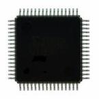
QFP-64
描述:
网络控制器与处理器 IC Neuron Chip w/ ext ROM I/F
Pictures:
3D模型
符号图
焊盘图
引脚图
产品图

TMPN3150B1AFG(I)数据手册
Page:
of 11 Go
若手册格式错乱,请下载阅览PDF原文件
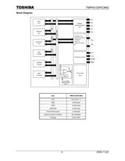
TMPN3120FE3MG
5 2005-11-29
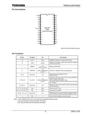
Pin Connections
Note: All NC pins should be open.
Pin Functions
Pin No. Pin Name I/O Pin Function
15 CLK1 Input Oscillator connection, or external clock input
14 CLK2 Output
Oscillator connection. Leave open when the external
clock is input to CLK1.
1 ~RESET
I/O
(built-in pull-up)
Reset pin (active low)
8 ~SERVICE
I/O
(built-in configurable
pull-up)
Service pin. Indicator output during operation.
7 to 4 IO
0
to IO
3
I/O
Large current sink capacity (20 mA)
General I/O port.
3, 30 to 28 IO
4
to IO
7
I/O
(built-in configurable
pull-up)
General I/O port. One of IO
4
to IO
7
can be specified as
the No.1 timer/counter input.
Output signals can be output to IO
0
.
IO
4
can be used as the No.2 timer/counter input with
IO
1
as output.
27, 26, 24 IO
8
to IO
10
I/O
General I/O port. Can be used for serial communication
with other devices.
2, 11, 12, 18, 25, 32 V
DD
Input Power input (5.0 V typ.)
9, 10, 13, 16, 23, 31 V
SS
Input Power input (0 V GND)
19, 20, 17, 21, 22 CP
0
to CP
4
I/O
Bidirectional port for communications. Supports several
communications protocols through specifying of mode.
― NC ― Do not connect anything. Leave pins open.
Note: ● The ~SERVICE and IO
4
to IO
7
terminals are programmable pull-ups.
● All V
DD
terminals must be externally connected.
● All V
SS
terminals must be externally connected.
TMPN3120FE3MG
器件 Datasheet 文档搜索
AiEMA 数据库涵盖高达 72,405,303 个元件的数据手册,每天更新 5,000 多个 PDF 文件
