Datasheet 搜索 > DSP数字信号处理器 > TI(德州仪器) > TMS320C25GBA 数据手册 > TMS320C25GBA 其他数据使用手册 2/4 页

¥ 1451.208
TMS320C25GBA 其他数据使用手册 - TI(德州仪器)
制造商:
TI(德州仪器)
分类:
DSP数字信号处理器
封装:
CPGA-68
描述:
TMS320第二代数字信号处理器 TMS320 SECOND GENERATION DIGITAL SIGNAL PROCESSORS
Pictures:
3D模型
符号图
焊盘图
引脚图
产品图
TMS320C25GBA数据手册
Page:
of 4 Go
若手册格式错乱,请下载阅览PDF原文件
Page 2
© 2003 BDTI (www.BDTI.com). All rights reserved.
tions. The level-one caches are fed by a
unified 64 Kbyte level-two memory. The
level-two memory can be configured as
SRAM, as a cache, or as a partitioned
combination of the two.
The TMS320C6713 on-chip memory
configuration is similar to that of the
TMS320C6711 and TMS320C6712,
except that it contains a larger 256 Kbyte
level-two memory.
Addressing
The TMS320C67x supports register-
direct and register-indirect addressing
modes and immediate data. In register-
indirect addressing mode, the address
register modification options include
pre-increment/decrement by a short (5-
bit) immediate or by the contents of any
general-purpose register, and post-incre-
ment/decrement by a short immediate or
by the contents of any general-purpose
register.
The TMS320C67x supports modulo
addressing. Up to eight registers (four
from each register file) can be config-
ured to operate under modulo address-
ing. The TMS320C67x does not support
bit-reversed addressing.
Pipeline
The TMS320C67x pipeline consists
of 16 stages. The pipeline is non-inter-
locked and is significantly deeper than
those of other commercially available
DSP processors.
Instructions are always fetched eight
at a time via the 256-bit instruction bus.
This group of eight instructions is called
a “fetch packet.” However, the
TMS320C67x cannot always execute
eight instructions in parallel. The group
of instructions to be executed in parallel
is called an “execution packet.” Because
the TMS320C67x supports variable-
length execution packets (and thus can
execute from one to eight instructions in
parallel), a single fetch packet may con-
tain several execution packets.
The processor does not check execu-
tion packets for resource contention.
Consequently, hand-written assembly
code may introduce resource conflicts
that produce unwanted behavior.
All branches on the TMS320C67x
are delayed branches with five delay
slots.
Most fixed-point instructions on the
TMS320C67x have a latency of one
cycle. The branch, fixed-point multiply,
and load instructions produce results
only after several cycles. Latencies for
floating point operations range from one
to ten cycles.
Instruction Set
The TMS320C62x uses an opcode-
operand assembly language format
where each instruction has an opcode
field for the operation and an operand
field for one to four operands. In addi-
tion, three optional fields can be used to
indicate parallel execution, conditional
execution, and the targeted execution
unit. If the target execution unit field is
omitted from the instruction, the assem-
bler attempts to select an appropriate
execution unit.
All instructions on the TMS320C67x
can be executed conditionally. Five des-
ignated general-purpose registers can be
used as condition registers.
The TMS320C67x does not support
hardware looping, so all loops must be
implemented in software. However, the
parallel architecture of the processor
allows the implementation of software
loops with virtually no overhead.
Due to its simple, RISC-like instruc-
tions, 32-bit instruction width, and uni-
form register sets, the instruction set of
the TMS320C67x is extremely regular
and straightforward.
Because the TMS320C67x is a
highly parallel architecture, obtaining
maximum performance often requires
the programmer to schedule instructions
carefully. This can be a challenge
because the TMS320C67x has a com-
plex architecture and long, variable
instruction latencies. Texas Instruments’
assembly optimizer tools and C compiler
simplify code development by automat-
ing the scheduling and parallelization
processes, but these tools do not always
result in optimal code.
Peripherals
TMS320C67x family members
include a variety of on-chip peripherals,
including a host port, a multi-channel
DMA controller, multi-channel buffered
serial ports, digital audio interfaces, and
32-bit timers.
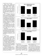
Benchmark Performance
The BDTI Benchmarks
TM
are a set of
DSP software functions that BDTI has
independently designed to provide an
objective basis for comparing processor
performance characteristics such as
speed and memory use for DSP applica-
tions. The BDTI Benchmark functions
are implemented in optimized assembly
language to allow a realistic assessment
of processors’ signal processing perfor-
mance. The resulting software is then
verified for functional correctness, opti-
mality, and adherence to the BDTI
Benchmark specifications. Benchmark
performance results are obtained either
through manual analysis and careful,
detailed simulation, or by measurement
on sample devices.
BDTI’s reports such as Buyer’s
Guide to DSP Processors and the Inside
series of reports include extensive BDTI
Benchmark results used to evaluate the
DSP performance of a set of processors.
For each benchmark, BDTI typically
reports cycle counts, execution time, a
cost-performance metric, an energy-effi-
ciency metric, and memory usage.
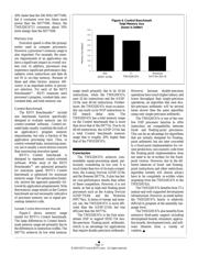
In this section, we present sample
execution time, cost-performance,
energy consumption, and memory usage
results taken from BDTI’s library of
benchmark results for the TMS320C67x
and two other floating-point processors:
the Analog Devices ADSP-2116x and
the Renesas (formerly Hitachi) SH775x,
which is based on the SH-4 core.
Execution Time
Execution time results in this report
were obtained assuming instructions and
data are preloaded in caches where appli-
cable. Processor speeds are for the fastest
available chips as of mid-2003.
器件 Datasheet 文档搜索
AiEMA 数据库涵盖高达 72,405,303 个元件的数据手册,每天更新 5,000 多个 PDF 文件
