Datasheet 搜索 > 微控制器 > TI(德州仪器) > TMS320F2811PBKA 数据手册 > TMS320F2811PBKA 其他数据使用手册 3/32 页
 器件3D模型
¥ 179.251
TMS320F2811PBKA 其他数据使用手册 - TI(德州仪器)
制造商:
TI(德州仪器)
分类:
微控制器
封装:
LQFP-128
描述:
TEXAS INSTRUMENTS TMS320F2811PBKA 芯片, 数字信号处理/控制器 带闪存, 32位
Pictures:
3D模型
符号图
焊盘图
引脚图
产品图
页面导航:
导航目录
TMS320F2811PBKA数据手册
Page:
of 32 Go
若手册格式错乱,请下载阅览PDF原文件
TMS320F28xx
和
TMS320F28xxx DSCs
的硬件设计指南
3ZHCA065–2008
年
8
月
www.ti.com.cn
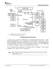
PWM
Interface/
Drivers
PWM
Load
Load�Power�Supply
18
External�Memory
High-
Current
switches
Actuators/
Relays
(FCE)
Keypad/
Display/
LEDs
Other
I/O
Devices
External
Interface
to�Digital
I/O�Pins
88
V
DDA18
XINTF
GPIO
(Pins�Multiplexed�with
Serial�Port,�PWM�and
Other�Signals)
V
DD
1.8�V
V
V
DDA2
DDAIO
3.3�VA
V
V
DDIO
DD3VFI
3.3�VD
Power�Management
Any�Other
Voltage�Rails
Comm.�Transceivers
(SCI,�SPI,�I2C,�CAN,�McBSP)
Signal
Conditioning
of Analog
Inputs
16
16
Analog
Inputs
Any�Other
Analog
Supply
3.3�V
V
IN
Crystal
or�Ext.
Oscillator
ADCINAx/Bx
PLL
Reset
Circuit
XRS/WD
TMS320F28xxx
Com�Ports
www.ti.com
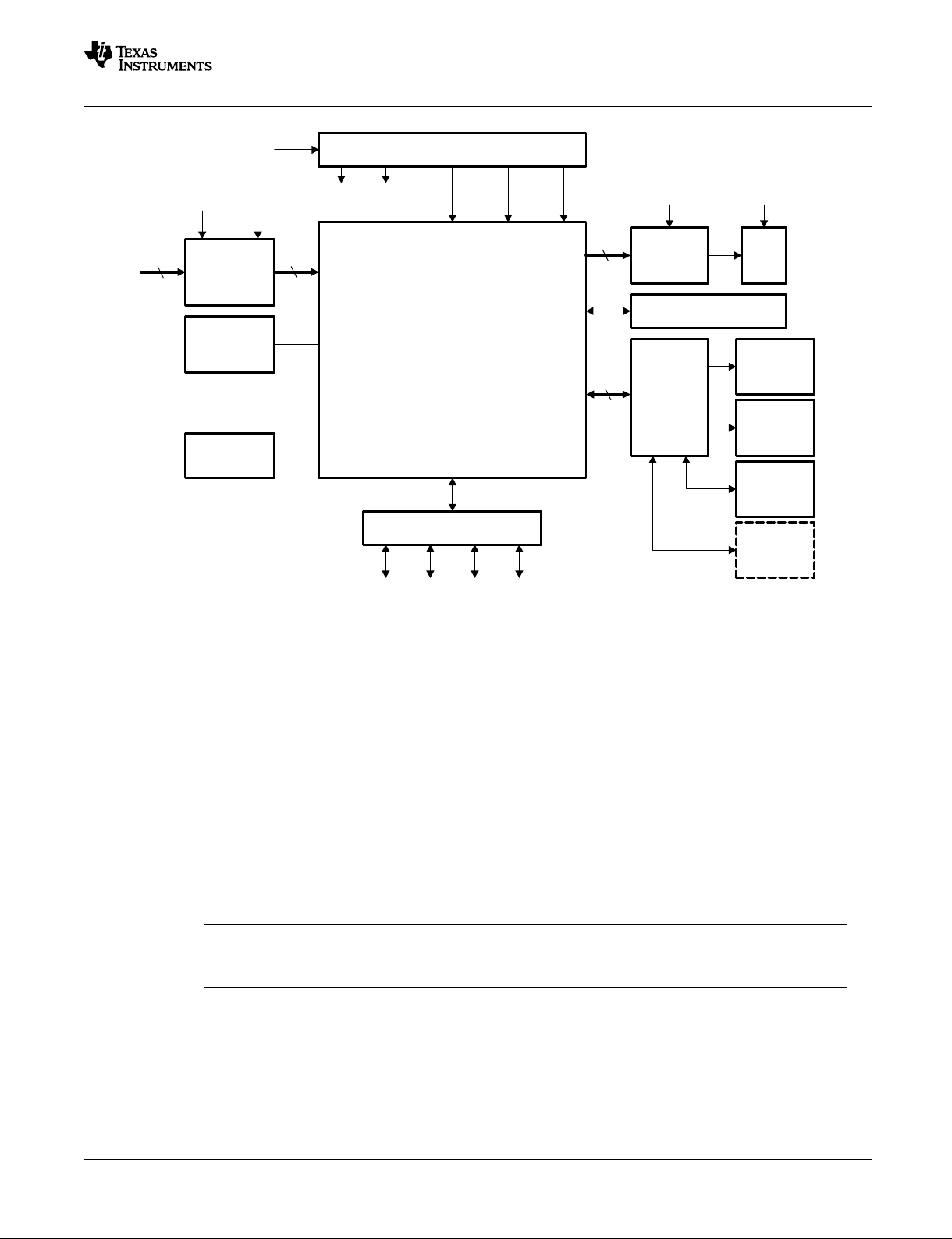
Typical System and Challenges
A External interface (XINTF) is available on the F2812 and F2833x devices only
B The maximum number of signals for any interface is device dependent.
Figure 1. Typical TMS320F28xx/28xxx System
TMS320F28xx/F28xxx devices include various onboard peripheral blocks. Though these peripherals save
adding external interface parts and make it flexible to meet the system level requirements for different
applications, it is challenging to design the hardware to operate all these peripherals and the DSC to
achieve the highest performance with optimum reliability. Therefore, designing a custom board, which
should work as desired on the first attempt, is a real challenge.
With the CPU frequency up to 150 MHz, there are many internal functional blocks onboard operating at
various frequencies. Any signal above 10 MHz can create a signal integrity issue if proper care is not
taken during schematics and layout design. In addition, there are low-level analog signals on the same
board. EMI/EMC and electrical noise issues should be considered before starting the board design.
Overall design must be debug friendly.
Note: This report considers the families TMS320F281x, F280x, F280xx and F2833x which are
active parts at the time of publication. Future revisions will include the data on newer parts.
SPRAAS1A– August 2008 Hardware Design Guidelines for TMS320F28xx and TMS320F28xxx DSCs 3
Submit Documentation Feedback
图
1.
典型的
TMS320F28xx/F28xxx
系统
A
外部接口尽在
F2812 and F2833x
芯片上可以得到
B
外部接口上的最大数字是因芯片的不同而定
.
TMS320F28xx/F28xxx
芯片包括了许多便携的外围设备,
虽然这些外设存储增加了部分外设接口,并且很容
易满足不同应用系统级的需要,但是,对于以操作所有外设为目的的硬件设计者,却带来了挑战,同时也给
数字信号控制器想以最大可信度得到最好的性能带来了挑战,所以,要想设计一块满足要求的电路板是很不
容易。随着
CPU
的频率上升到
150MHz
,有许多内部功能时钟需要在不同频率下工作。如果在原理图和布线
设计阶段不采取一些措施的话,任何超过
10MHz
的信号都可能产生信号干扰问题。
同时,由于在电路板上存在低电压的模拟信号,所以电磁的干扰和兼容,以及电磁噪声,在开始设计电路板
时都要考虑到。再有,整体设计必须有利于友好调试功能。
本指导书只考虑到了在当前出版物上比较常见的
TMS320F281x, F280x, F280xx
和
F2833x
系列,
将来的指
导书将要包括新的型号的芯片
注释:
典型的系统和存在的问题
器件 Datasheet 文档搜索
AiEMA 数据库涵盖高达 72,405,303 个元件的数据手册,每天更新 5,000 多个 PDF 文件
