Datasheet 搜索 > 微处理器 > AMD(超微半导体) > CS5536AD B1 数据手册 > CS5536AD B1 产品设计参考手册 1/36 页

 器件3D模型
¥ 30.344
CS5536AD B1 产品设计参考手册 - AMD(超微半导体)
制造商:
AMD(超微半导体)
分类:
微处理器
封装:
PBGA
Pictures:
3D模型
符号图
焊盘图
引脚图
产品图
页面导航:
引脚图在P11Hot
典型应用电路图在P35
原理图在P1
封装尺寸在P36
型号编码规则在P36
功能描述在P1P11
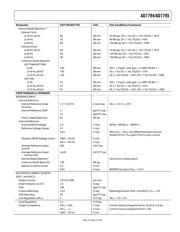
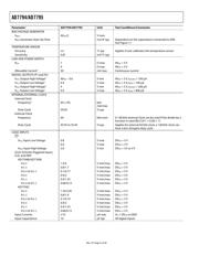
技术参数、封装参数在P1P3P4P10P13P19
应用领域在P1P35
电气规格在P16
导航目录
CS5536AD B1数据手册
Page:
of 36 Go
若手册格式错乱,请下载阅览PDF原文件
6-Channel, Low Noise, Low Power, 24-/16-Bit
∑-Δ ADC with On-Chip In-Amp and Reference
AD7794/AD7795
Rev. D
Information furnished by Analog Devices is believed to be accurate and reliable. However, no
responsibility is assumed by Analog Devices for its use, nor for any infringements of patents or other
rights of third parties that may result from its use. Specifications subject to change without notice. No
license is granted by implication or otherwise under any patent or patent rights of Analog Devices.
Trademarks and registered trademarks are the property of their respective owners.
One Technology Way, P.O. Box 9106, Norwood, MA 02062-9106, U.S.A.
Tel: 781.329.4700 www.analog.com
Fax: 781.461.3113 ©2004–2007 Analog Devices, Inc. All rights reserved.
FEATURES
Up to 23 effective bits
RMS noise: 40 nV @ 4.17 Hz, 85 nV @ 16.7 Hz
Current: 400 μA typical
Power-down: 1 μA maximum
Low noise, programmable gain, instrumentation amp
Band gap reference with 4 ppm/°C drift typical
Update rate: 4.17 Hz to 470 Hz
Six differential analog inputs
Internal clock oscillator
Simultaneous 50 Hz/60 Hz rejection
Reference detect
Programmable current sources
On-chip bias voltage generator
Burnout currents
Low-side power switch
Power supply: 2.7 V to 5.25 V
Temperature range:
B grade: –40°C to +105°C
C grade: –40°C to +125°C
Independent interface power supply
24-lead TSSOP
3-wire serial interface
SPI®, QSPI™, MICROWIRE™, and DSP compatible
Schmitt trigger on SCLK
APPLICATIONS
Temperature measurement
Pressure measurement
Weigh scales
Strain gage transducers
Gas analysis
Industrial process control
Instrumentation
Blood analysis
Smart transmitters
Liquid/gas chromatography
6-digit DVM
GENERAL DESCRIPTION
The AD7794/AD7795 are low power, low noise, complete
analog front ends for high precision measurement applications.
They contain a low noise, 24-/16-bit ∑-Δ ADC with six
differential inputs. The on-chip low noise instrumentation
amplifier means that signals of small amplitude can be
interfaced directly to the ADC.
Each device contains a precision, low noise, low drift internal
band gap reference, and can also accept up to two external
differential references. Other on-chip features include
programmable excitation current sources, burnout currents,
and a bias voltage generator that is used to set the common-
mode voltage of a channel to AV
DD
/2. The low-side power
switch can be used to power down bridge sensors between
conversions, minimizing the system’s power consumption. The
AD7794/AD7795 can operate with either an internal clock or
an external clock. The output data rate from each part can vary
from 4.17 Hz to 470 Hz.
Both parts operate with a power supply from 2.7 V to 5.25 V.
The B-grade parts (AD7794 and AD7795) are specified for a
temperature range of −40°C to +105°C while the C-grade part
(AD7794) is specified for a temperature range of −40°C to
+125°C. They consume a current of 400 μA typical and are
housed in a 24-lead TSSOP.
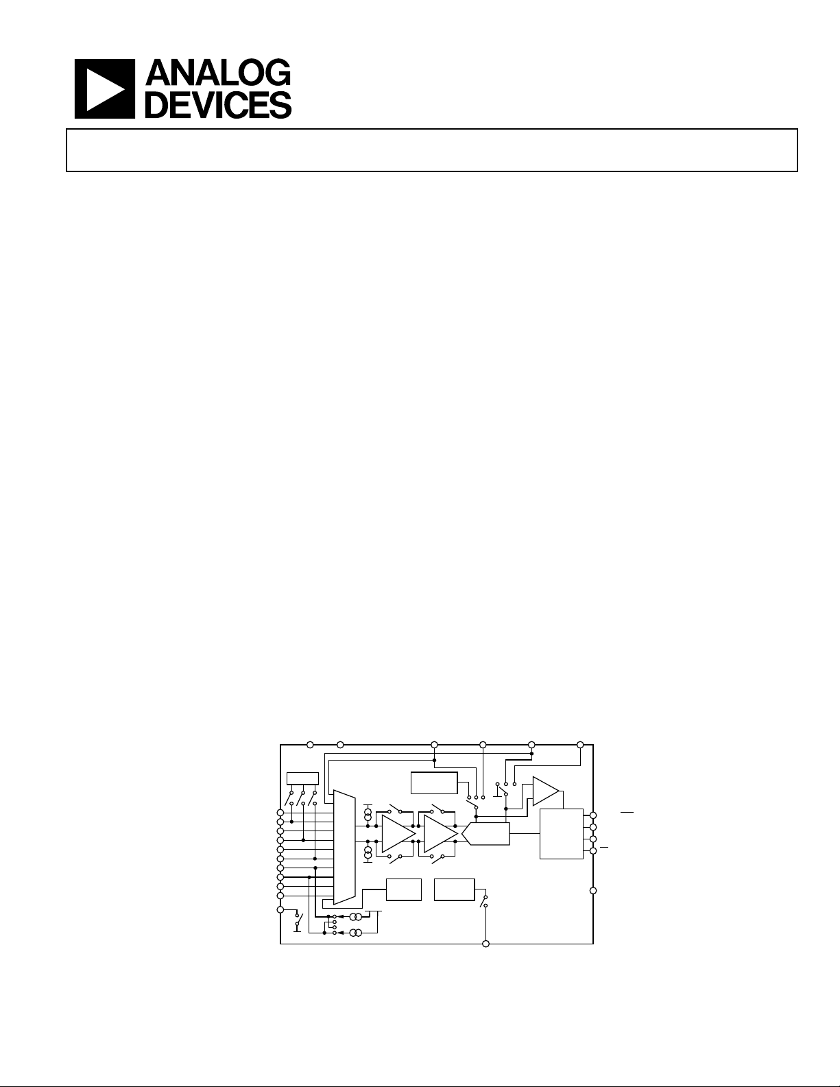
FUNCTIONAL BLOCK DIAGRAM
04854-001
DOUT/RD
Y
DIN
SCLK
CS
DV
DD
SERIAL
INTERFACE
AND
LOGIC
CONTROL
Σ-Δ
ADC
AD7794: 24-BIT ADC
AD7795: 16-BIT ADC
AD7794/AD7795
AIN1(+)
AIN1(–)
AIN2(+)
AIN2(–)
AIN3(+)
AIN3(–)
A
IN5(+)/IOUT2
A
IN5(–)/IOUT1
AIN6(+)/P1
AIN6(–)/P2
V
DD
GND
MUX
V
BIAS
PSW
GND
BAND GAP
REFERENCE
TEMP
SENSOR
CLK
INTERNAL
CLOCK
GND
REFERENCE
DETECT
GND A
V
DD
A
IN4(+)
/
REFIN2(+) REFIN1(+)
A
IN4(
–
)
/
REFIN2(
–
) REFIN1(
–
)
V
DD
IN-AMPBUF
Figure 1.
器件 Datasheet 文档搜索
AiEMA 数据库涵盖高达 72,405,303 个元件的数据手册,每天更新 5,000 多个 PDF 文件
