Datasheet 搜索 > MOS管 > TI(德州仪器) > CSD87355Q5D 数据手册 > CSD87355Q5D 产品设计参考手册 1/19 页

¥ 16.772
CSD87355Q5D 产品设计参考手册 - TI(德州仪器)
制造商:
TI(德州仪器)
分类:
MOS管
封装:
LSON-CLIP
描述:
CSD87355Q5D 同步降压 NexFET™ 电源块
Pictures:
3D模型
符号图
焊盘图
引脚图
产品图
页面导航:
原理图在P4
技术参数、封装参数在P3
应用领域在P19
导航目录
CSD87355Q5D数据手册
Page:
of 19 Go
若手册格式错乱,请下载阅览PDF原文件
User's Guide
SLUU416A–May 2010–Revised September 2010
CSD86350Q5DEVM-604
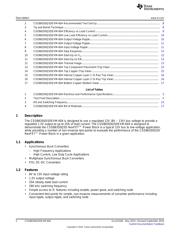
The CSD86350Q5DEVM-604 evaluation module (EVM) is a synchronous buck converter featuring TI's
NexFET™ Power Block technology to provide a high current, ultra-high density power supply solution. The
EVM provides a 1.2V output at 25A from a 12V nominal input bus at over 92% efficiency. The EVM is
designed to operate from a single supply, so no additional bias voltage is required. The EVM uses the
TPS51218 high performance, mid-input voltage, synchronous buck controller and TI’s NexFET™ Power
Block to optimize the efficiency and power density of the total solution.
Contents
1 Description ................................................................................................................... 2
1.1 Applications ......................................................................................................... 2
1.2 Features ............................................................................................................. 2
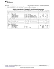
2 CSD86350Q5DEVM-604 Electrical Performance Specifications ..................................................... 3
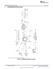
3 CSD86350Q5DEVM-604 Schematic ..................................................................................... 4
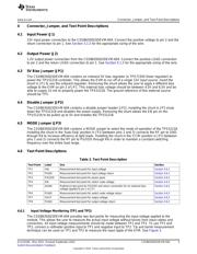
4 Connector, Jumper, and Test Point Descriptions ....................................................................... 5
4.1 Input Power (J1) .................................................................................................... 5
4.2 Output Power (J2) ................................................................................................. 5
4.3 5V Bias Jumper (JP1) ............................................................................................. 5
4.4 Disable Jumper (JP2) ............................................................................................. 5
4.5 MODE Jumper (JP3) .............................................................................................. 5
4.6 Test Point Descriptions ............................................................................................ 5
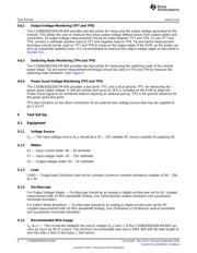
5 Test Set Up .................................................................................................................. 6
5.1 Equipment ........................................................................................................... 6
5.2 Equipment Setup ................................................................................................... 7
5.3 Start Up/Shut Down Procedure .................................................................................. 8
5.4 Output Ripple Voltage Measurement Procedure .............................................................. 9
5.5 Equipment Shutdown .............................................................................................. 9
6 CSD86350Q5DEVM-604 Test Data ...................................................................................... 9
6.1 Efficiency ............................................................................................................ 9
6.2 Efficiency (Low Load) ............................................................................................ 10
6.3 Output Voltage Ripple ........................................................................................... 10
6.4 Output Voltage Ripple ........................................................................................... 11
6.5 Input Voltage Ripple .............................................................................................. 11
6.6 Load Transient Response ....................................................................................... 12
6.7 Start Up on V
IN
.................................................................................................... 12
6.8 Start Up on EN .................................................................................................... 13
6.9 Thermal Image .................................................................................................... 13
7 CSD86350Q5DEVM-604 Modifications ................................................................................ 13
7.1 Switching Frequency ............................................................................................. 14
7.2 Output Voltage .................................................................................................... 14
7.3 Gate Drive Resistors ............................................................................................. 14
8 CSD86350Q5DEVM-604 Assembly Drawings and Layout .......................................................... 14
9 CSD86350Q5DEVM-604 Bill of Materials .............................................................................. 17
List of Figures
1 CSD86350Q5DEVM-604 Schematic ..................................................................................... 4
NexFET is a trademark of Texas Instruments.
1
SLUU416A–May 2010–Revised September 2010 CSD86350Q5DEVM-604
Submit Documentation Feedback
Copyright © 2010, Texas Instruments Incorporated
器件 Datasheet 文档搜索
AiEMA 数据库涵盖高达 72,405,303 个元件的数据手册,每天更新 5,000 多个 PDF 文件
