Datasheet 搜索 > 32位控制器 > NXP(恩智浦) > LPC2148FBD64 数据手册 > LPC2148FBD64 产品设计参考手册 4/354 页
 器件3D模型
¥ 152.556
LPC2148FBD64 产品设计参考手册 - NXP(恩智浦)
制造商:
NXP(恩智浦)
分类:
32位控制器
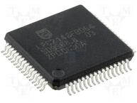
封装:
LQFP-64
描述:
NXP LPC2148FBD64 微控制器(MCU), 16/32位, ARM7, 512K闪存, 64LQFP
Pictures:
3D模型
符号图
焊盘图
引脚图
产品图
页面导航:
引脚图在P22P23P28P45P48P50P51P52P53P54P55P56Hot
原理图在P7P75P271P321P325
功能描述在P150P166
应用领域在P4P49P58P80P206P228P229P230P231P232P234P245
导航目录
LPC2148FBD64数据手册
Page:
of 354 Go
若手册格式错乱,请下载阅览PDF原文件

UM10139 All information provided in this document is subject to legal disclaimers. © NXP B.V. 2012. All rights reserved.
User manual Rev. 4 — 23 April 2012 4 of 354
NXP Semiconductors
UM10139
Chapter 1: Introductory information
• 60 MHz maximum CPU clock available from programmable on-chip PLL with settling
time of 100 s.
• On-chip integrated oscillator operates with an external crystal in range from 1 MHz to
30 MHz and with an external oscillator up to 50 MHz.
• Power saving modes include Idle and Power-down.
• Individual enable/disable of peripheral functions as well as peripheral clock scaling for
additional power optimization.
• Processor wake-up from Power-down mode via external interrupt, USB, Brown-Out
Detect (BOD) or Real-Time Clock (RTC).
• Single power supply chip with Power-On Reset (POR) and BOD circuits:
– CPU operating voltage range of 3.0 V to 3.6 V (3.3 V 10 %) with 5 V tolerant I/O
pads.
1.3 Applications
• Industrial control
• Medical systems
• Access control
• Point-of-sale
• Communication gateway
• Embedded soft modem
• General purpose applications
1.4 Device information
[1] While the USB DMA is the primary user of the additional 8 kB RAM, this RAM is also accessible at any time by the CPU as a general
purpose RAM for data and code storage.
1.5 Architectural overview
The LPC2141/2/4/6/8 consists of an ARM7TDMI-S CPU with emulation support, the
ARM7 Local Bus for interface to on-chip memory controllers, the AMBA Advanced
High-performance Bus (AHB) for interface to the interrupt controller, and the ARM
Table 1. LPC2141/2/4/6/8 device information
Device Number
of pins
On-chip
SRAM
Endpoint
USB RAM
On-chip
FLASH
Number of
10-bit ADC
channels
Number of
10-bit DAC
channels
Note
LPC2141 64 8kB 2kB 32kB 6 - -
LPC2142 64 16 kB 2 kB 64 kB 6 1 -
LPC2144 64 16 kB 2 kB 128 kB 14 1 UART1 with full
modem interface
LPC2146 64 32 kB + 8 kB
[1]
2 kB 256 kB 14 1 UART1 with full
modem interface
LPC2148 64 32 kB + 8 kB
[1]
2 kB 512 kB 14 1 UART1 with full
modem interface
器件 Datasheet 文档搜索
AiEMA 数据库涵盖高达 72,405,303 个元件的数据手册,每天更新 5,000 多个 PDF 文件
