Datasheet 搜索 > 32位控制器 > NXP(恩智浦) > LPC2148FBD64 数据手册 > LPC2148FBD64 产品设计参考手册 6/354 页
 器件3D模型
¥ 152.477
LPC2148FBD64 产品设计参考手册 - NXP(恩智浦)
制造商:
NXP(恩智浦)
分类:
32位控制器
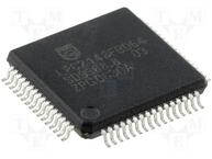
封装:
LQFP-64
描述:
NXP LPC2148FBD64 微控制器(MCU), 16/32位, ARM7, 512K闪存, 64LQFP
Pictures:
3D模型
符号图
焊盘图
引脚图
产品图
页面导航:
引脚图在P22P23P28P45P48P50P51P52P53P54P55P56Hot
原理图在P7P75P271P321P325
功能描述在P150P166
应用领域在P4P49P58P80P206P228P229P230P231P232P234P245
导航目录
LPC2148FBD64数据手册
Page:
of 354 Go
若手册格式错乱,请下载阅览PDF原文件

UM10139 All information provided in this document is subject to legal disclaimers. © NXP B.V. 2012. All rights reserved.
User manual Rev. 4 — 23 April 2012 6 of 354
NXP Semiconductors
UM10139
Chapter 1: Introductory information
1.7 On-chip flash memory system
The LPC2141/2/4/6/8 incorporate a 32 kB, 64 kB, 128 kB, 256 kB, and 512 kB Flash
memory system, respectively. This memory may be used for both code and data storage.
Programming of the Flash memory may be accomplished in several ways: over the serial
built-in JTAG interface, using In System Programming (ISP) and UART0, or by means of
In Application Programming (IAP) capabilities. The application program, using the IAP
functions, may also erase and/or program the Flash while the application is running,
allowing a great degree of flexibility for data storage field firmware upgrades, etc. When
the LPC2141/2/4/6/8 on-chip bootloader is used, 32 kB, 64 kB, 128 kB, 256 kB, and
500 kB of Flash memory is available for user code.
The LPC2141/2/4/6/8 Flash memory provides minimum of 100,000 erase/write cycles and
20 years of data-retention.
1.8 On-chip Static RAM (SRAM)
On-chip Static RAM (SRAM) may be used for code and/or data storage. The on-chip
SRAM may be accessed as 8-bits, 16-bits, and 32-bits. The LPC2141/2/4/6/8 provide
8/16/32 kB of static RAM, respectively.
The LPC2141/2/4/6/8 SRAM is designed to be accessed as a byte-addressed memory.
Word and halfword accesses to the memory ignore the alignment of the address and
access the naturally-aligned value that is addressed (so a memory access ignores
address bits 0 and 1 for word accesses, and ignores bit 0 for halfword accesses).
Therefore valid reads and writes require data accessed as halfwords to originate from
addresses with address line 0 being 0 (addresses ending with 0, 2, 4, 6, 8, A, C, and E in
hexadecimal notation) and data accessed as words to originate from addresses with
address lines 0 and 1 being 0 (addresses ending with 0, 4, 8, and C in hexadecimal
notation). This rule applies to both off and on-chip memory usage.
The SRAM controller incorporates a write-back buffer in order to prevent CPU stalls
during back-to-back writes. The write-back buffer always holds the last data sent by
software to the SRAM. This data is only written to the SRAM when another write is
requested by software (the data is only written to the SRAM when software does another
write). If a chip reset occurs, actual SRAM contents will not reflect the most recent write
request (i.e. after a "warm" chip reset, the SRAM does not reflect the last write operation).
Any software that checks SRAM contents after reset must take this into account. Two
identical writes to a location guarantee that the data will be present after a Reset.
Alternatively, a dummy write operation before entering idle or power-down mode will
similarly guarantee that the last data written will be present in SRAM after a subsequent
Reset.
器件 Datasheet 文档搜索
AiEMA 数据库涵盖高达 72,405,303 个元件的数据手册,每天更新 5,000 多个 PDF 文件
