Datasheet 搜索 > 微处理器 > TI(德州仪器) > OMAP3530DCUSA 数据手册 > OMAP3530DCUSA 产品设计参考手册 6/265 页

 器件3D模型
¥ 342.239
OMAP3530DCUSA 产品设计参考手册 - TI(德州仪器)
制造商:
TI(德州仪器)
分类:
微处理器
封装:
FCBGA-423
Pictures:
3D模型
符号图
焊盘图
引脚图
产品图
页面导航:
引脚图在P6P14Hot
原理图在P5P177P178P179
封装尺寸在P259P260
标记信息在P259P260
封装信息在P4P256P257P258P259P260P261
功能描述在P196
技术参数、封装参数在P4P121P134P135P136P137P138P139P140P141P142P143
应用领域在P1P2P3P4P5P6P7P10P11P12P13P14
电气规格在P4P119P120P121P122P123P124P125P126P127P128P129


导航目录
OMAP3530DCUSA数据手册
Page:
of 265 Go
若手册格式错乱,请下载阅览PDF原文件

OMAP3530, OMAP3525
SPRS507H –FEBRUARY 2008–REVISED OCTOBER 2013
www.ti.com
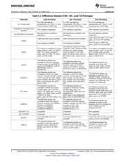
Table 1-1. Differences Between CBB, CBC, and CUS Packages
FEATURE CBB PACKAGE CBC PACKAGE CUS PACKAGE
For CBB package pin For CBC package pin For CUS package pin
Pin Assignments assignments see Table 2-1, Ball assignments see Table 2-2, Ball assignments see Table 2-3, Ball
Characteristics (CBB Pkg.) Characteristics (CBC Pkg.) Characteristics (CUS Pkg.)
Package-On-Package (POP)
POP interface supported POP interface supported POP interface not available
Interface
Discrete Memory Interface Discrete Memory Interface not Discrete Memory Interface
Discrete Memory Interface
supported supported supported
Chip-select pins gpmc_ncs1 and
Eight chip-select pins available Eight chip-select pins available
gpmc_ncs2 are not available
GPMC
Wait pins gpmc_wait1 and
Four wait pins available Four wait pins available
gpmc_wait2 are not available
The following signals are either
CTS signal is available on 3 pins available on two (double muxed) CTS signal is available on 3 pins
(triple muxed): uart1_cts (AG22 / or three pins (triple muxed): (triple muxed): uart1_cts (AC19 /
UART1 W8 / T21), uart1_rts (AH22 / uart1_cts (AE21 / T19 / W2), AC2 / AA18), uart1_rts (W6 /
AA9), uart1_tx (F28 / Y8 / AE7), uart1_rts (AE22 / R2), uart1_rx AB19), uart1_tx (E23 / V7 / AC3),
uart1_rx (E26 / AA8) (H3 / H25 / AE4), uart1_tx (L4 / uart1_rx (D24 / W7)
G26)
The following signals are
The following signals are
available on two pins (double The following signals are
available on two pins (double
muxed): uart2_cts (AF6/AB26), available on one pin only:
UART2 muxed): uart2_cts (Y24/P3),
uart2_rts (AE6/AB25), uart2_tx uart2_cts (V6), uart2_rts (V5),
uart2_rts (AA24/N3), uart2_tx
(AF5/AA25), uart2_rx uart2_tx (W4), uart2_rx (V4)
(AD22/U3), uart2_rx (AD21/W3)
(AE5/AD25)
The following signals are The following signals are
The following signals are
available on three pins (triple available on two pins (triple
available on two pins only
muxed): mcbsp3_dx (AF6 / AB26 muxed): mcbsp3_dx (U17/ Y24/
(double muxed): mcbsp3_dx
McBSP3 / V21), mcbsp3_dr (AE6 / AB25 / P3), mcbsp3_dr (T20/ AA24 /
(V6/W18), mcbsp3_dr (V5/Y18),
U21), mcbsp3_clkx (AF5 / AA25 / N3), mcbsp3_clkx (T17/ AD22 /
mcbsp3_clkx (W4/V18), and
W21), and mcbsp3_fsx (AE5 / U3), mcbsp3_fsx (P20/ AD21 /
mcbsp3_fsx (V4/AA19)
AD25 / K26) W3)
The following signals are The following signals are
The following signals are
available on three pins (triple available on three pins (triple
available on two pins only
muxed): gpt8_pwm_evt (N8 / muxed): gpt8_pwm_evt
(double muxed): gpt8_pwm_evt
GP Timer AD25 / V3), gpt9_pwm_evt (T8 / (C5/AD21/V9), gpt9_pwm_evt
(G4/M4), gpt9_pwm_evt (F4/N4),
AB26 / Y2), gpt10_pwm_evt (R8 (B4/W8/Y24),
gpt10_pwm_evt (G5/N3), and
/ AB25 / Y3), and gpt10_pwm_evt(C4/U8/AA24),
gpt11_pwm_evt (F3/M5)
gpt11_pwm_evt (P8 / AA25 / Y4) gpt11_pwm_evt(B5/V8/AD22)
The following signals are The following signals are
The following signals are
available on two pins (double available on two pins (double
available on one pin only:
muxed): mcbsp4_clkx (T8/AE1), muxed): mcbsp4_clkx (B4 / V3),
McBSP4 mcbsp4_clkx (F4), mcbsp4_dr
mcbsp4_dr (R8/AD1), mcbsp4_dr (C4 / U4),
(G5), mcbsp4_dx (F3),
mcbsp4_dx (P8/AD2), mcbsp4_dx (B5 / R3),
mcbsp4_fsx (G4)
mcbsp4_fsx (N8/AC1) mcbsp4_fsx (C5 / T3)
HSUSB3_TLL Supported Supported Not supported
MM_FSUSB3 Supported Supported Not supported
Four chip-select pins are Four chip-select pins are Chip-select pins mcspi1_cs1 and
McSPI1
available available mcspi_cs2 are not available
The following signals are
The following signals are The following signals are
available on two pins (double
available on two pins (double available on one pin only:
MMC3 muxed): mmc3_cmd (AC3 /
muxed): mmc3_cmd (R8 / AB3), mmc3_cmd (AD3), and
AE10), and mmc3_clk (AB1 /
mmc3_clk (R9 / AB2) mmc3_clk (AC1)
AF10)
6 OMAP3530 and OMAP3525 Applications Processors Copyright © 2008–2013, Texas Instruments Incorporated
Submit Documentation Feedback
Product Folder Links: OMAP3530 OMAP3525
器件 Datasheet 文档搜索
AiEMA 数据库涵盖高达 72,405,303 个元件的数据手册,每天更新 5,000 多个 PDF 文件
