Datasheet 搜索 > 微控制器 > TI(德州仪器) > TMS320F2812PGFA 数据手册 > TMS320F2812PGFA 产品设计参考手册 2/178 页
 器件3D模型
¥ 67.007
TMS320F2812PGFA 产品设计参考手册 - TI(德州仪器)
制造商:
TI(德州仪器)
分类:
微控制器
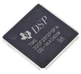
封装:
LQFP-176
描述:
TEXAS INSTRUMENTS TMS320F2812PGFA 芯片, 数字信号处理器 150MHz SMD
Pictures:
3D模型
符号图
焊盘图
引脚图
产品图
页面导航:
引脚图在P14P15P16Hot
典型应用电路图在P38P80
原理图在P26P42P60P64P69P79P82
封装尺寸在P163P164P167P174
焊盘布局在P168P175
标记信息在P163P164
封装信息在P13P163P164P165
功能描述在P10P12P13P17P18P19P20P21P22P23P24P25
技术参数、封装参数在P35P36P91P92P93P94P95P96P97P98P99P100
应用领域在P27P28P29P51P144P165
电气规格在P17P36P91P92P93P94P95P96P97P98P99P100
导航目录
TMS320F2812PGFA数据手册
Page:
of 178 Go
若手册格式错乱,请下载阅览PDF原文件

TMS320F2810, TMS320F2811, TMS320F2812
TMS320C2810, TMS320C2811, TMS320C2812
www.ti.com
SPRS174T –APRIL 2001–REVISED MAY 2012
Contents
1 TMS320F281x, TMS320C281x DSPs ..................................................................................... 10
1.1 Features .................................................................................................................... 10
1.2 Getting Started ............................................................................................................. 11
2 Introduction ...................................................................................................................... 12
2.1 Description ................................................................................................................. 12
2.2 Device Summary .......................................................................................................... 13
2.3 Pin Assignments ........................................................................................................... 14
2.3.1 Terminal Assignments for the GHH/ZHH Packages ....................................................... 14
2.3.2 Pin Assignments for the PGF Package ...................................................................... 15
2.3.3 Pin Assignments for the PBK Package ...................................................................... 16
2.4 Signal Descriptions ........................................................................................................ 17
3 Functional Overview .......................................................................................................... 26
3.1 Memory Map ............................................................................................................... 27
3.2 Brief Descriptions .......................................................................................................... 32
3.2.1 C28x CPU ....................................................................................................... 32
3.2.2 Memory Bus (Harvard Bus Architecture) .................................................................... 32
3.2.3 Peripheral Bus .................................................................................................. 32
3.2.4 Real-Time JTAG and Analysis ................................................................................ 33
3.2.5 External Interface (XINTF) (2812 Only) ...................................................................... 33
3.2.6 Flash (F281x Only) ............................................................................................. 33
3.2.7 ROM (C281x Only) ............................................................................................. 33
3.2.8 M0, M1 SARAMs ............................................................................................... 34
3.2.9 L0, L1, H0 SARAMs ............................................................................................ 34
3.2.10 Boot ROM ....................................................................................................... 34
3.2.11 Security .......................................................................................................... 34
3.2.12 Peripheral Interrupt Expansion (PIE) Block ................................................................. 36
3.2.13 External Interrupts (XINT1, XINT2, XINT13, XNMI) ........................................................ 36
3.2.14 Oscillator and PLL .............................................................................................. 36
3.2.15 Watchdog ........................................................................................................ 36
3.2.16 Peripheral Clocking ............................................................................................. 36
3.2.17 Low-Power Modes .............................................................................................. 36
3.2.18 Peripheral Frames 0, 1, 2 (PFn) .............................................................................. 37
3.2.19 General-Purpose Input/Output (GPIO) Multiplexer ......................................................... 37
3.2.20 32-Bit CPU-Timers (0, 1, 2) ................................................................................... 37
3.2.21 Control Peripherals ............................................................................................. 37
3.2.22 Serial Port Peripherals ......................................................................................... 38
3.3 Register Map ............................................................................................................... 39
3.4 Device Emulation Registers .............................................................................................. 41
3.5 External Interface, XINTF (2812 Only) ................................................................................. 42
3.5.1 Timing Registers ................................................................................................ 43
3.5.2 XREVISION Register ........................................................................................... 43
3.6 Interrupts .................................................................................................................... 44
3.6.1 External Interrupts .............................................................................................. 47
3.7 System Control ............................................................................................................ 48
3.8 OSC and PLL Block ....................................................................................................... 50
3.8.1 Loss of Input Clock ............................................................................................. 51
3.9 PLL-Based Clock Module ................................................................................................ 52
3.10 External Reference Oscillator Clock Option ........................................................................... 52
3.11 Watchdog Block ........................................................................................................... 53
3.12 Low-Power Modes Block ................................................................................................. 54
4 Peripherals ....................................................................................................................... 55
2 Contents Copyright © 2001–2012, Texas Instruments Incorporated
器件 Datasheet 文档搜索
AiEMA 数据库涵盖高达 72,405,303 个元件的数据手册,每天更新 5,000 多个 PDF 文件
