Datasheet 搜索 > 微控制器 > TI(德州仪器) > TMS320F2812PGFA 数据手册 > TMS320F2812PGFA 产品设计参考手册 3/178 页
 器件3D模型
¥ 67.07
TMS320F2812PGFA 产品设计参考手册 - TI(德州仪器)
制造商:
TI(德州仪器)
分类:
微控制器
封装:
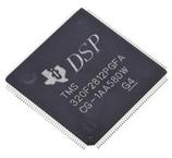
LQFP-176
描述:
TEXAS INSTRUMENTS TMS320F2812PGFA 芯片, 数字信号处理器 150MHz SMD
Pictures:
3D模型
符号图
焊盘图
引脚图
产品图
页面导航:
引脚图在P14P15P16Hot
典型应用电路图在P38P80
原理图在P26P42P60P64P69P79P82
封装尺寸在P163P164P167P174
焊盘布局在P168P175
标记信息在P163P164
封装信息在P13P163P164P165
功能描述在P10P12P13P17P18P19P20P21P22P23P24P25
技术参数、封装参数在P35P36P91P92P93P94P95P96P97P98P99P100
应用领域在P27P28P29P51P144P165
电气规格在P17P36P91P92P93P94P95P96P97P98P99P100
导航目录
TMS320F2812PGFA数据手册
Page:
of 178 Go
若手册格式错乱,请下载阅览PDF原文件

TMS320F2810, TMS320F2811, TMS320F2812
TMS320C2810, TMS320C2811, TMS320C2812
www.ti.com
SPRS174T –APRIL 2001–REVISED MAY 2012
4.1 32-Bit CPU-Timers 0/1/2 ................................................................................................. 55
4.2 Event Manager Modules (EVA, EVB) ................................................................................... 58
4.2.1 General-Purpose (GP) Timers ................................................................................ 61
4.2.2 Full-Compare Units ............................................................................................. 61
4.2.3 Programmable Deadband Generator ........................................................................ 61
4.2.4 PWM Waveform Generation .................................................................................. 61
4.2.5 Double Update PWM Mode ................................................................................... 61
4.2.6 PWM Characteristics ........................................................................................... 62
4.2.7 Capture Unit ..................................................................................................... 62
4.2.8 Quadrature-Encoder Pulse (QEP) Circuit ................................................................... 62
4.2.9 External ADC Start-of-Conversion ........................................................................... 62
4.3 Enhanced Analog-to-Digital Converter (ADC) Module ............................................................... 63
4.4 Enhanced Controller Area Network (eCAN) Module .................................................................. 68
4.5 Multichannel Buffered Serial Port (McBSP) Module .................................................................. 73
4.6 Serial Communications Interface (SCI) Module ....................................................................... 77
4.7 Serial Peripheral Interface (SPI) Module ............................................................................... 80
4.8 GPIO MUX ................................................................................................................. 83
5 Development Support ........................................................................................................ 86
5.1 Device and Development Support Tool Nomenclature ............................................................... 86
5.2 Documentation Support .................................................................................................. 87
5.3 Community Resources .................................................................................................... 89
6 Electrical Specifications ..................................................................................................... 91
6.1 Absolute Maximum Ratings .............................................................................................. 91
6.2 Recommended Operating Conditions .................................................................................. 91
6.3 Electrical Characteristics Over Recommended Operating Conditions (Unless Otherwise Noted) ............. 92
6.4 Current Consumption ..................................................................................................... 93
6.5 Current Consumption Graphs ............................................................................................ 95
6.6 Reducing Current Consumption ......................................................................................... 97
6.7 Emulator Connection Without Signal Buffering for the DSP ......................................................... 97
6.8 Power Sequencing Requirements ....................................................................................... 98
6.9 Signal Transition Levels ................................................................................................. 100
6.10 Timing Parameter Symbology .......................................................................................... 101
6.11 General Notes on Timing Parameters ................................................................................ 101
6.12 Test Load Circuit ......................................................................................................... 101
6.13 Device Clock Table ...................................................................................................... 102
6.14 Clock Requirements and Characteristics ............................................................................. 103
6.14.1 Input Clock Requirements ................................................................................... 103
6.14.2 Output Clock Characteristics ................................................................................ 104
6.15 Reset Timing ............................................................................................................. 104
6.16 Low-Power Mode Wakeup Timing ..................................................................................... 108
6.17 Event Manager Interface ................................................................................................ 112
6.17.1 PWM Timing ................................................................................................... 112
6.17.2 Interrupt Timing ................................................................................................ 114
6.18 General-Purpose Input/Output (GPIO) – Output Timing ............................................................ 115
6.19 General-Purpose Input/Output (GPIO) – Input Timing .............................................................. 116
6.20 Serial Peripheral Interface (SPI) Master Mode Timing .............................................................. 117
6.21 Serial Peripheral Interface (SPI) Slave Mode Timing ............................................................... 122
6.22 External Interface (XINTF) Timing ..................................................................................... 126
6.23 XINTF Signal Alignment to XCLKOUT ................................................................................ 130
6.24 External Interface Read Timing ........................................................................................ 131
6.25 External Interface Write Timing ........................................................................................ 133
6.26 External Interface Ready-on-Read Timing With One External Wait State ....................................... 134
6.27 External Interface Ready-on-Write Timing With One External Wait State ....................................... 137
Copyright © 2001–2012, Texas Instruments Incorporated Contents 3
器件 Datasheet 文档搜索
AiEMA 数据库涵盖高达 72,405,303 个元件的数据手册,每天更新 5,000 多个 PDF 文件
