Datasheet 搜索 > 微控制器 > TI(德州仪器) > TMS320F28334ZJZQ 数据手册 > TMS320F28334ZJZQ 产品设计参考手册 3/199 页
 器件3D模型
¥ 155.529
TMS320F28334ZJZQ 产品设计参考手册 - TI(德州仪器)
制造商:
TI(德州仪器)
分类:
微控制器
封装:
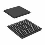
BGA-176
描述:
数字信号控制器(DSC ) Digital Signal Controllers (DSCs)
Pictures:
3D模型
符号图
焊盘图
引脚图
产品图
页面导航:
引脚图在P14P79P80Hot
典型应用电路图在P48P95
原理图在P33P58P65P73P75P78P87P94P97P100P106
封装尺寸在P189P190P191
标记信息在P189P190P191P192
封装信息在P11P12P13P189P190P191P192
技术参数、封装参数在P45P46P116P117P118P119P120P121P122P123P124P125
应用领域在P61P113P140P199
电气规格在P46P116P117P118P119P120P121P122P123P124P125P126
导航目录
TMS320F28334ZJZQ数据手册
Page:
of 199 Go
若手册格式错乱,请下载阅览PDF原文件

TMS320F28335, TMS320F28334, TMS320F28332
TMS320F28235, TMS320F28234, TMS320F28232
www.ti.com
SPRS439M –JUNE 2007–REVISED AUGUST 2012
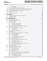
4.7.2 ADC Registers .................................................................................................. 82
4.7.3 ADC Calibration ................................................................................................. 83
4.8 Multichannel Buffered Serial Port (McBSP) Module .................................................................. 83
4.9 Enhanced Controller Area Network (eCAN) Modules (eCAN-A and eCAN-B) .................................... 86
4.10 Serial Communications Interface (SCI) Modules (SCI-A, SCI-B, SCI-C) .......................................... 91
4.11 Serial Peripheral Interface (SPI) Module (SPI-A) ..................................................................... 95
4.12 Inter-Integrated Circuit (I2C) ............................................................................................. 98
4.13 GPIO MUX ................................................................................................................. 99
4.14 External Interface (XINTF) .............................................................................................. 106
5 Device Support ................................................................................................................ 108
5.1 Device and Development Support Tool Nomenclature ............................................................. 108
5.2 Documentation Support ................................................................................................. 110
5.3 Community Resources .................................................................................................. 115
6 Electrical Specifications ................................................................................................... 116
6.1 Absolute Maximum Ratings ............................................................................................ 116
6.2 Recommended Operating Conditions ................................................................................. 117
6.3 Electrical Characteristics ................................................................................................ 117
6.4 Current Consumption .................................................................................................... 118
6.4.1 Reducing Current Consumption ............................................................................. 120
6.4.2 Current Consumption Graphs ............................................................................... 121
6.4.3 Thermal Design Considerations ............................................................................. 122
6.5 Emulator Connection Without Signal Buffering for the DSP ....................................................... 123
6.6 Timing Parameter Symbology .......................................................................................... 124
6.6.1 General Notes on Timing Parameters ...................................................................... 124
6.6.2 Test Load Circuit .............................................................................................. 124
6.6.3 Device Clock Table ........................................................................................... 125
6.7 Clock Requirements and Characteristics ............................................................................. 126
6.8 Power Sequencing ....................................................................................................... 127
6.8.1 Power Management and Supervisory Circuit Solutions .................................................. 128
6.9 General-Purpose Input/Output (GPIO) ................................................................................ 131
6.9.1 GPIO - Output Timing ........................................................................................ 131
6.9.2 GPIO - Input Timing .......................................................................................... 132
6.9.3 Sampling Window Width for Input Signals ................................................................. 133
6.9.4 Low-Power Mode Wakeup Timing .......................................................................... 134
6.10 Enhanced Control Peripherals ......................................................................................... 139
6.10.1 Enhanced Pulse Width Modulator (ePWM) Timing ....................................................... 139
6.10.2 Trip-Zone Input Timing ....................................................................................... 139
6.10.3 High-Resolution PWM Timing ............................................................................... 140
6.10.4 Enhanced Capture (eCAP) Timing ......................................................................... 140
6.10.5 Enhanced Quadrature Encoder Pulse (eQEP) Timing ................................................... 141
6.10.6 ADC Start-of-Conversion Timing ............................................................................ 142
6.11 External Interrupt Timing ................................................................................................ 142
6.12 I2C Electrical Specification and Timing ............................................................................... 143
6.13 Serial Peripheral Interface (SPI) Timing .............................................................................. 143
6.13.1 Master Mode Timing .......................................................................................... 143
6.13.2 SPI Slave Mode Timing ...................................................................................... 148
6.14 External Interface (XINTF) Timing ..................................................................................... 151
6.14.1 USEREADY = 0 ............................................................................................... 151
6.14.2 Synchronous Mode (USEREADY = 1, READYMODE = 0) ............................................. 152
6.14.3 Asynchronous Mode (USEREADY = 1, READYMODE = 1) ............................................ 153
6.14.4 XINTF Signal Alignment to XCLKOUT ..................................................................... 155
6.14.5 External Interface Read Timing ............................................................................. 156
6.14.6 External Interface Write Timing ............................................................................. 158
Copyright © 2007–2012, Texas Instruments Incorporated Contents 3
器件 Datasheet 文档搜索
AiEMA 数据库涵盖高达 72,405,303 个元件的数据手册,每天更新 5,000 多个 PDF 文件
