Datasheet 搜索 > 微控制器 > TI(德州仪器) > TMS320F28335PTPQ 数据手册 > TMS320F28335PTPQ 产品设计参考手册 2/199 页
 器件3D模型
¥ 79.813
TMS320F28335PTPQ 产品设计参考手册 - TI(德州仪器)
制造商:
TI(德州仪器)
分类:
微控制器
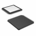
封装:
LQFP-176
描述:
TEXAS INSTRUMENTS TMS320F28335PTPQ 芯片, 数字信号控制器, LQFP-176
Pictures:
3D模型
符号图
焊盘图
引脚图
产品图
页面导航:
引脚图在P14P79P80Hot
典型应用电路图在P48P95
原理图在P33P58P65P73P75P78P87P94P97P100P106
封装尺寸在P189P190P191
标记信息在P189P190P191P192
封装信息在P11P12P13P189P190P191P192
技术参数、封装参数在P45P46P116P117P118P119P120P121P122P123P124P125
应用领域在P61P113P140P199
电气规格在P46P116P117P118P119P120P121P122P123P124P125P126
导航目录
TMS320F28335PTPQ数据手册
Page:
of 199 Go
若手册格式错乱,请下载阅览PDF原文件

TMS320F28335, TMS320F28334, TMS320F28332
TMS320F28235, TMS320F28234, TMS320F28232
www.ti.com
SPRS439M –JUNE 2007–REVISED AUGUST 2012
Contents
1 TMS320F2833x, TMS320F2823x DSCs .................................................................................. 10
1.1 Features .................................................................................................................... 10
1.2 Getting Started ............................................................................................................. 11
2 Introduction ...................................................................................................................... 12
2.1 Pin Assignments ........................................................................................................... 14
2.2 Signal Descriptions ........................................................................................................ 23
3 Functional Overview .......................................................................................................... 33
3.1 Memory Maps .............................................................................................................. 34
3.2 Brief Descriptions .......................................................................................................... 41
3.2.1 C28x CPU ....................................................................................................... 41
3.2.2 Memory Bus (Harvard Bus Architecture) .................................................................... 41
3.2.3 Peripheral Bus .................................................................................................. 41
3.2.4 Real-Time JTAG and Analysis ................................................................................ 42
3.2.5 External Interface (XINTF) .................................................................................... 42
3.2.6 Flash ............................................................................................................. 42
3.2.7 M0, M1 SARAMs ............................................................................................... 42
3.2.8 L0, L1, L2, L3, L4, L5, L6, L7 SARAMs ..................................................................... 43
3.2.9 Boot ROM ........................................................................................................ 43
3.2.9.1 Peripheral Pins Used by the Bootloader ........................................................ 44
3.2.10 Security .......................................................................................................... 44
3.2.11 Peripheral Interrupt Expansion (PIE) Block ................................................................. 46
3.2.12 External Interrupts (XINT1–XINT7, XNMI) .................................................................. 46
3.2.13 Oscillator and PLL .............................................................................................. 46
3.2.14 Watchdog ........................................................................................................ 46
3.2.15 Peripheral Clocking ............................................................................................. 46
3.2.16 Low-Power Modes .............................................................................................. 46
3.2.17 Peripheral Frames 0, 1, 2, 3 (PFn) ........................................................................... 47
3.2.18 General-Purpose Input/Output (GPIO) Multiplexer ......................................................... 47
3.2.19 32-Bit CPU-Timers (0, 1, 2) ................................................................................... 47
3.2.20 Control Peripherals ............................................................................................. 48
3.2.21 Serial Port Peripherals ......................................................................................... 48
3.3 Register Map ............................................................................................................... 49
3.4 Device Emulation Registers .............................................................................................. 51
3.5 Interrupts .................................................................................................................... 52
3.5.1 External Interrupts .............................................................................................. 56
3.6 System Control ............................................................................................................ 57
3.6.1 OSC and PLL Block ............................................................................................ 58
3.6.1.1 External Reference Oscillator Clock Option .................................................... 59
3.6.1.2 PLL-Based Clock Module ......................................................................... 60
3.6.1.3 Loss of Input Clock ................................................................................ 61
3.6.2 Watchdog Block ................................................................................................. 62
3.7 Low-Power Modes Block ................................................................................................. 63
4 Peripherals ....................................................................................................................... 64
4.1 DMA Overview ............................................................................................................. 64
4.2 32-Bit CPU-Timer 0, CPU-Timer 1, CPU-Timer 2 ..................................................................... 66
4.3 Enhanced PWM Modules ................................................................................................ 68
4.4 High-Resolution PWM (HRPWM) ....................................................................................... 72
4.5 Enhanced CAP Modules ................................................................................................. 73
4.6 Enhanced QEP Modules ................................................................................................. 75
4.7 Analog-to-Digital Converter (ADC) Module ............................................................................ 77
4.7.1 ADC Connections if the ADC Is Not Used .................................................................. 81
2 Contents Copyright © 2007–2012, Texas Instruments Incorporated
器件 Datasheet 文档搜索
AiEMA 数据库涵盖高达 72,405,303 个元件的数据手册,每天更新 5,000 多个 PDF 文件
