Datasheet 搜索 > DA转换器 > ADI(亚德诺) > AD9832BRU 数据手册 > AD9832BRU 用户编程技术手册 2/29 页

 器件3D模型
¥ 63.182
AD9832BRU 用户编程技术手册 - ADI(亚德诺)
制造商:
ADI(亚德诺)
分类:
DA转换器
封装:
TSSOP-16
描述:
CMOS DDS完成 CMOS Complete DDS
Pictures:
3D模型
符号图
焊盘图
引脚图
产品图
页面导航:
导航目录
AD9832BRU数据手册
Page:
of 29 Go
若手册格式错乱,请下载阅览PDF原文件

AD9832 Data Sheet
Rev. E | Page 2 of 28
TABLE OF CONTENTS
Features .............................................................................................. 1
Applications ....................................................................................... 1
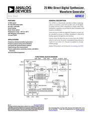
General Description ......................................................................... 1
Functional Block Diagram .............................................................. 1
Revision History ............................................................................... 2
Specifications ..................................................................................... 3
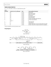
Timing Characteristics ................................................................ 5
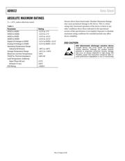
Absolute Maximum Ratings ............................................................ 6
ESD Caution .................................................................................. 6
Pin Configuration and Function Descriptions ............................. 7
Typical Performance Characteristics ............................................. 8
Terminology .................................................................................... 11
Theory of Operation ...................................................................... 12
Circuit Description ......................................................................... 13
Numerical Controlled Oscillator and Phase Modulator ....... 13
Sine Look-Up Table (LUT) ........................................................ 13
Digital-to-Analog Converter .................................................... 13
Functional Description .................................................................. 14
Serial Interface ............................................................................ 14
Direct Data Transfer and Deferred Data Transfer ................. 14
Latency ......................................................................................... 16
Flowcharts ................................................................................... 16
Applications Information .............................................................. 19
Grounding and Layout .............................................................. 19
Interfacing the AD9832 to Microprocessors .............................. 19
AD9832 to ADSP-2101 Interface ............................................. 19
AD9832 to 68HC11/68L11 Interface ....................................... 20
AD9832 to 80C51/80L51 Interface .......................................... 20
AD9832 to DSP56002 Interface ............................................... 20
Evaluation Board ............................................................................ 21
System Demonstration Platform .............................................. 21
AD9832 to SPORT Interface ..................................................... 21
XO vs. External Clock ................................................................ 21
Power Supply ............................................................................... 21
Evaluation Board Schematics ................................................... 22
Evaluation Board Layout ........................................................... 24
Ordering Information .................................................................... 25
Bill of Materials ........................................................................... 25
Outline Dimensions ....................................................................... 26
Ordering Guide .......................................................................... 26
REVISION HISTORY
2/13—Rev. D to Rev. E
Changes to Table 10 ........................................................................ 15
Changes to Flowcharts Section ..................................................... 16
7/12—Rev. C to Rev. D
Changed On-Chip COS Lookup Table to On-Chip SIN Lookup
Table in Features Section ................................................................. 1
9/11—Rev. B to Rev. C
Changes to Features and Applications ........................................... 1
Changes to Specification Statement ............................................... 3
Changes to Timing Characteristics Statement ............................. 5
Replaced Evaluation Board Section; Renumbered
Sequentially ..................................................................................... 21
Changes to Ordering Guide .......................................................... 26
6/10—Rev. A to Rev. B
Updated Format .................................................................. Universal
Changed CMOS Complete DDS to 3 V to 5.0 V Programmable
Waveform Generator......................................................................... 1
Changes to Serial Interface Section.............................................. 14
Updated Outline Dimensions ....................................................... 23
Changes to Ordering Guide .......................................................... 23
7/99—Rev 0 to Rev. A
器件 Datasheet 文档搜索
AiEMA 数据库涵盖高达 72,405,303 个元件的数据手册,每天更新 5,000 多个 PDF 文件
