Datasheet 搜索 > RF射频器件 > Microchip(微芯) > ATMEGA1284RFR2-ZF 数据手册 > ATMEGA1284RFR2-ZF 用户编程技术手册 6/607 页
 器件3D模型
¥ 19.534
ATMEGA1284RFR2-ZF 用户编程技术手册 - Microchip(微芯)
制造商:
Microchip(微芯)
分类:
RF射频器件
封装:
VQFN-48
Pictures:
3D模型
符号图
焊盘图
引脚图
产品图
页面导航:
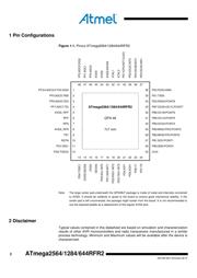
引脚图在P2P5P219P256P274P339Hot
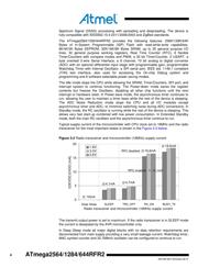
典型应用电路图在P87P179P538
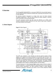
原理图在P3P9P33P46P80P82P85P87P96P192P217P256
型号编码规则在P591P592P593
封装信息在P594
功能描述在P67P361
技术参数、封装参数在P81P95P105P110P550P561P563
应用领域在P1P97P181P207P243P247P485P502P503P538P552
电气规格在P77P180P190P204P205P217P234P235P444P446P550P554

导航目录
ATMEGA1284RFR2-ZF数据手册
Page:
of 607 Go
若手册格式错乱,请下载阅览PDF原文件

6
42073B-MCU Wireless-09/14
ATmega2564/1284/644RFR2
source current if the pull-up resistors are activated. The Port E pins are tri-stated when
a reset condition becomes active, even if the clock is not running.
Due to the low pin count of the QFN48 package port E6 is not connected to a pin.
Port E also provides functions of various special features of the
ATmega2564/1284/644RFR2.
3.2.10 Port F (PF7..PF5,PF4/3,PF2...PF0)
Internally Port F is an 8-bit bi-directional I/O port with internal pull-up resistors (selected
for each bit). The Port F output buffers have symmetrical drive characteristics with both
high sink and source capability. As inputs, Port F pins that are externally pulled low will
source current if the pull-up resistors are activated. The Port F pins are tri-stated when
a reset condition becomes active, even if the clock is not running.
Due to the low pin count of the QFN48 package port F3 and F4 are connected to the
same pin. The I/O configuration should be done carefully in order to avoid excessive
power dissipation.
Port F also provides functions of various special features of the
ATmega2564/1284/644RFR2.
3.2.11 Port G (PG4,PG3,PG1)
Internally Port G is a 6-bit bi-directional I/O port with internal pull-up resistors (selected
for each bit). The Port G output buffers have symmetrical drive characteristics with both
high sink and source capability. However the driver strength of PG3 and PG4 is
reduced compared to the other port pins. The output voltage drop (V
OH
, V
OL
) is higher
while the leakage current is smaller. As inputs, Port G pins that are externally pulled low
will source current if the pull-up resistors are activated. The Port G pins are tri-stated
when a reset condition becomes active, even if the clock is not running.
Due to the low pin count of the QFN48 package port G0, G2 and G5 are not connected
to a pin.
Port G also provides functions of various special features of the
ATmega2564/1284/644RFR2.
3.2.12 AVSS_RFP
AVSS_RFP is a dedicated ground pin for the bi-directional, differential RF I/O port.
3.2.13 AVSS_RFN
AVSS_RFN is a dedicated ground pin for the bi-directional, differential RF I/O port.
3.2.14 RFP
RFP is the positive terminal for the bi-directional, differential RF I/O port.
3.2.15 RFN
RFN is the negative terminal for the bi-directional, differential RF I/O port.
3.2.16 RSTN
Reset input. A low level on this pin for longer than the minimum pulse length will
generate a reset, even if the clock is not running. Shorter pulses are not guaranteed to
generate a reset.
3.2.17 XTAL1
Input to the inverting 16MHz crystal oscillator amplifier. In general a crystal between
XTAL1 and XTAL2 provides the 16MHz reference clock of the radio transceiver.
3.2.18 XTAL2
Output of the inverting 16MHz crystal oscillator amplifier.
器件 Datasheet 文档搜索
AiEMA 数据库涵盖高达 72,405,303 个元件的数据手册,每天更新 5,000 多个 PDF 文件
