Datasheet 搜索 > LVDS、M-LVDS、ECL、CML > TI(德州仪器) > DS90C032WGLQMLV 数据手册 > DS90C032WGLQMLV 用户编程技术手册 3/12 页
 器件3D模型
¥ 2409.788
DS90C032WGLQMLV 用户编程技术手册 - TI(德州仪器)
制造商:
TI(德州仪器)
分类:
LVDS、M-LVDS、ECL、CML
封装:
SOP
描述:
DS90C032QML LVDS四通道CMOS差分线路接收器 DS90C032QML LVDS Quad CMOS Differential Line Receiver
Pictures:
3D模型
符号图
焊盘图
引脚图
产品图
页面导航:
导航目录
DS90C032WGLQMLV数据手册
Page:
of 12 Go
若手册格式错乱,请下载阅览PDF原文件
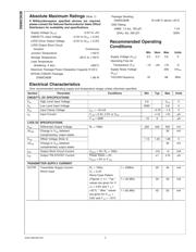
Electrical Characteristics (Continued)
Over recommended operating supply and temperature ranges unless otherwise specified.
Symbol Parameter Conditions Min Typ Max Units
TRANSMITTER SUPPLY CURRENT
ICCTG Transmitter Supply Current
16 Grayscale
R
L
= 100Ω,
C
L
= 5 pF,
16 Grayscale Pattern
(Figures 2, 4 ) " Typ "
values are given for V
CC
= 3.6V and T
A
=
+25˚C, " Max " values
are given for V
CC
=
3.6V and T
A
= −10˚C
f = 25 MHz 28 40 mA
f = 40 MHz 32 45 mA
f = 65 MHz 39 50 mA
ICCTZ Transmitter Supply Current
Power Down
Power Down = Low
Driver Outputs in TRI-STATE
®
under
Power Down Mode
11 150 µA
Note 1: “Absolute Maximum Ratings” are those values beyond which the safety of the device cannot be guaranteed. They are not meant to imply that the device
should be operated at these limits. The tables of “Electrical Characteristics” specify conditions for device operation.
Note 2: Typical values are given for V
CC
= 3.3V and T
A
= +25˚C unless specified otherwise.
Note 3: Current into device pins is defined as positive. Current out of device pins is defined as negative. Voltages are referenced to ground unless otherwise
specified (except V
OD
and ∆V
OD
).
Note 4: V
OS
previously referred as V
CM
.
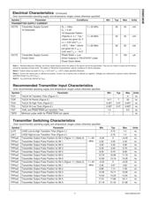
Recommended Transmitter Input Characteristics
Over recommended operating supply and temperature ranges unless otherwise specified
Symbol Parameter Min Typ Max Units
TCIT TxCLK IN Transition Time (Figure 5 ) 5ns
TCIP TxCLK IN Period (Figure 6 ) 14.7 T 50 ns
TCIH TxCLK IN High Time (Figure 6 ) 0.35T 0.5T 0.65T ns
TCIL TxCLK IN Low Time (Figure 6 ) 0.35T 0.5T 0.65T ns
TXIT TxIN, and Power Down pin transition Time
1.5 6.0 ns
TXPD Minimum pulse width for Power Down pin signal
1us
Transmitter Switching Characteristics
Over recommended operating supply and temperature ranges unless otherwise specified
Symbol Parameter Min Typ Max Units
LLHT LVDS Low-to-High Transition Time (Figure 4 ) 0.75 1.4 ns
LHLT LVDS High-to-Low Transition Time (Figure 4 ) 0.75 1.4 ns
TPPos0 Transmitter Output Pulse Position for Bit 0 (Figure 11 ) (Note 5) f = 65
MHz
−0.20 0 +0.20 ns
TPPos1 Transmitter Output Pulse Position for Bit 1 2.00 2.20 2.40 ns
TPPos2 Transmitter Output Pulse Position for Bit 2 4.20 4.40 4.60 ns
TPPos3 Transmitter Output Pulse Position for Bit 3 6.39 6.59 6.79 ns
TPPos4 Transmitter Output Pulse Position for Bit 4 8.59 8.79 8.99 ns
TPPos5 Transmitter Output Pulse Position for Bit 5 10.79 10.99 11.19 ns
TPPos6 Transmitter Output Pulse Position for Bit 6 12.99 13.19 13.39 ns
TPPos0 Transmitter Output Pulse Position for Bit 0 (Figure 11 ) (Note 5) f = 40
MHz
−0.25 0 +0.25 ns
TPPos1 Transmitter Output Pulse Position for Bit 1 3.32 3.57 3.82 ns
TPPos2 Transmitter Output Pulse Position for Bit 2 6.89 7.14 7.39 ns
TPPos3 Transmitter Output Pulse Position for Bit 3 10.46 10.71 10.96 ns
TPPos4 Transmitter Output Pulse Position for Bit 4 14.04 14.29 14.54 ns
TPPos5 Transmitter Output Pulse Position for Bit 5 17.61 17.86 18.11 ns
TPPos6 Transmitter Output Pulse Position for Bit 6 21.18 21.43 21.68 ns
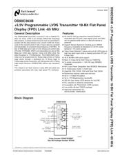
DS90C363B
www.national.com3
器件 Datasheet 文档搜索
AiEMA 数据库涵盖高达 72,405,303 个元件的数据手册,每天更新 5,000 多个 PDF 文件
