Datasheet 搜索 > FPGA芯片 > Microsemi(美高森美) > FLASHPRO5 数据手册 > FLASHPRO5 用户编程技术手册 2/4 页

¥ 384.692
FLASHPRO5 用户编程技术手册 - Microsemi(美高森美)
制造商:
Microsemi(美高森美)
分类:
FPGA芯片
Pictures:
3D模型
符号图
焊盘图
引脚图
产品图
页面导航:
功能描述在P3
导航目录
FLASHPRO5数据手册
Page:
of 4 Go
若手册格式错乱,请下载阅览PDF原文件

Microcontroller
5-32
small sector sizes (from 64 to 512 bytes, depending on the
memory density), the RAM requirements are much less
than those of large sector Flash devices. The latter gener-
ally have 4 K to 128K byte sector sizes.
A second advantage of Atmel’s Flash is that an entire sec-
tor can be updated during a single program operation,
instead of the byte-by-byte programming of previous gener-
ation Flash memories. This saves significant programming
time when updating an entire sector, especially when com-
paring Atmel’s small sector devices with large sector
devices. In addition, Atmel’s devices do not require a sector
erase prior to writing, thus saving additional programming
time. The maximum sector program time is 10 ms and 20
ms for the AT29Cxxx and AT29LVxxx/AT29BVxxx families
respectively.
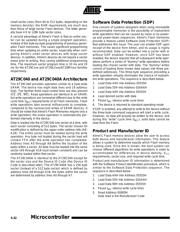
AT29C040 and AT29C040A Architecture
The AT29C040 provides operation similar to a byte-wide
SRAM. The device has eight data lines and 19 address
lines. The familiar three input control lines are also present
(CE
, OE, WE). Read operations are identical to an SRAM,
but write operations are somewhat different due to the write
cycle time (t
WC
) requirements of all Flash memories. Flash
write operations take several milliseconds to complete,
compared to the nanosecond writes of SRAM devices. It
should be noted that Atmel’s Flash Memories require only a
write operation; the erase operation is automatically per-
formed internally in the device.
Data is loaded into the AT29C040 one sector at a time, with
each sector consisting of 512 bytes. The sector chosen for
modification is defined by the upper order address bits (A9-
A18). The entire sector must be loaded during the write
operation. Any byte not loaded during the sector load will
contain FFH after the write operation has completed.
Address lines A0 through A8 define the location of the
bytes within a sector. All data must be loaded into the same
sector (A9 through A18 must remain constant) and can be
randomly loaded within that sector.
The AT29C040A is identical to the AT29C040 except for
the sector size and the Device ID Code (the Device ID
Code is described later). The AT29C040A has a 256 byte
sector (instead of a 512 byte sector) which is defined by
address lines A8 through A18; the bytes within the sector
are determined by address lines A0 through A7.
Software Data Protection (SDP)
One concern of systems designers when using nonvolatile
programmable memories is the possibility of inadvertent
write operations that can be caused by noise or by power-
up and power-down sequences. Atmel’s Flash memories
provide a feature called Software Data Protection (SDP)
that addresses this issue. The user can enable SDP upon
receipt of the device from Atmel, and its usage is highly
recommended. Data can be written into a sector with or
without SDP enabled. However, once SDP has been
enabled, the device requires that all subsequent write oper-
ations perform a series of “dummy” write operations before
loading the chosen sector with data. The “dummy” writes
consist of loading three known data values into three pre-
defined addresses. This three-byte sequence preceding a
write operation virtually eliminates the chance of inadvert-
ent write operations. The sequence is described below.
1. Load Data AAH into Address 05555H
2. Load Data 55H into Address 02AAAH
3. Load Data A0H into Address 05555H
4. Load desired sector with data
5. Pause t
WC
(device write cycle time)
6. The device is returned to standard operating mode
If SDP is enabled, any attempt to write to the device without
the three-byte command sequence will start a write cycle.
However, no data will actually be written to the device, and
during this “write” cycle time (t
WC
), valid data cannot be
read from the Flash.
Product and Manufacturer ID
Atmel’s Flash memory devices allow the user to access
both device and manufacturer information. This feature
allows a system to determine exactly which Flash memory
is being used. Once this is known, the host system can
choose different algorithms for write operations in order to
accommodate for differences in device density, V
CC
requirements, sector size, and required write cycle time.
Product and manufacturer ID information is determined
with the Software Product Identification procedure, which is
similar to the Software Data Protection sequence. The
sequence is described below.
1. Load Data AAH into Address 05555H
2. Load Data 55H into Address 02AAAH
3. Load Data 90H into Address 05555H
4. Pause t
WC
(device write cycle time)
5. Read Address 00000H
Data read is the Manufacturer Code
器件 Datasheet 文档搜索
AiEMA 数据库涵盖高达 72,405,303 个元件的数据手册,每天更新 5,000 多个 PDF 文件


