Datasheet 搜索 > 微控制器 > NXP(恩智浦) > MC68HC908QT1VPE 数据手册 > MC68HC908QT1VPE 用户编程技术手册 5/32 页
 器件3D模型
¥ 15.051
MC68HC908QT1VPE 用户编程技术手册 - NXP(恩智浦)
制造商:
NXP(恩智浦)
分类:
微控制器
封装:
DIP-8
Pictures:
3D模型
符号图
焊盘图
引脚图
产品图
MC68HC908QT1VPE数据手册
Page:
of 32 Go
若手册格式错乱,请下载阅览PDF原文件

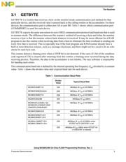
The Routines
Using MC68HC908 On-Chip FLASH Programming Routines, Rev. 3
Freescale Semiconductor 5
used in conjunction with RDVRRNG to perform a complete program and verification cycle of the specified
range.
PRGRNGE allows any range to be passed to it. That is, the range does not have to be coincident with row
boundaries
1
. The range specified can be at the beginning of a row, the middle of a row, the end of a row,
or it can be a range overlapping row boundaries. The user must ensure only two things:
• The range specified is first erased
• The data for the specified range must be in the data array in RAM
Because this routine calls the delay routine DELNUS to generate proper delays, parameter CPUSPD must
be set correctly when calling PRGRNGE. Parameters required for this routine are explained in more detail
later in Section 5, “Variables.”
Interrupts are masked (the I bit is set) and COP is serviced in this routine.
NOTE
Regarding the JB8 and JL/JKxx(E), the FLASH block protect register
(FLBPR) dose not consist of FLASH. Since FLASH is always protected
after reset, unprotect the locations to be programmed in the user software
before calling this routine.
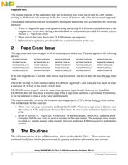
3.4 ERARNGE — Page Erase
The page erase operation using the ERARNGE routine supports the following devices:
If the user target device is not in the above list, refer to Section 2, “Page Erase Issue.”
ERARNGE can be called to erase a page of FLASH. This routine does not use the last address (LADDR)
variable. The first address (FADDR) placed in H:X in the two previous routines actually can be any address
within a page to be erased. To select the page erase operation, a control variable in RAM called CTRLBYT
is used. Writing $00 to CTRLBYT selects the page erase operation. To set proper delays, CPUSPD must
be set correctly. CPUSPD and CTRLBYT are explained in more detail later in Section 5, “Variables.”
Interrupts are masked. In the EY16 and GT16 ERARNGE, COP is not serviced. On the other hand in the
QT/QYxx ERARNGE, COP is serviced. Servicing COP does not cause the page erase issue for these
devices.
Regarding the MC68HLC908QT/QYxx devices, only 1 MHz operating frequency (f
op
) is supported so
that CPUSPD must be set with a value $04.
1. The flexible boundary condition does not apply for the MC68HLC908QT/QYxx devices. When FLASH is programmed using
this routine for these devices, all bytes that will be programmed must be in the same row. Furthermore, only a 1 MHz operating
frequency (f
op
) is supported so that CPUSPD must be set with a value $04. COP is not serviced.
MC68HC908EY16 MC68HC908GT16 MC68HC908QT1 MC68HC908QT2 MC68HC908QT4
MC68HC908QY1 MC68HC908QY2 MC68HC908QY4 MC68HLC908QT1 MC68HLC908QT2
MC68HLC908QT4 MC68HLC908QY1 MC68HLC908QY2 MC68HLC908QY4
器件 Datasheet 文档搜索
AiEMA 数据库涵盖高达 72,405,303 个元件的数据手册,每天更新 5,000 多个 PDF 文件
