Datasheet 搜索 > 微处理器 > NXP(恩智浦) > MPC8313CVRAFFC 数据手册 > MPC8313CVRAFFC 用户编程技术手册 4/28 页
 器件3D模型
¥ 593.706
MPC8313CVRAFFC 用户编程技术手册 - NXP(恩智浦)
制造商:
NXP(恩智浦)
分类:
微处理器
封装:
PBGA-516
描述:
NXP MPC8313CVRAFFC 芯片, 微控制器, 32位, POWER, 333MHZ, TEPBGA-II-516
Pictures:
3D模型
符号图
焊盘图
引脚图
产品图
MPC8313CVRAFFC数据手册
Page:
of 28 Go
若手册格式错乱,请下载阅览PDF原文件
Programming the User-Programmable Machine (UPM) for SDRAM Memory Devices, Rev. 0
4 Freescale Semiconductor
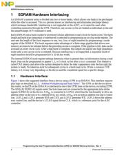
SDRAM Hardware Interfacing
NOTE
Figure 1 shows that addressing requires glue logic on the board. Section 1.2,
“Address Multiplexing and Bank Select,” explains the need for the glue
logic and how to implement it.
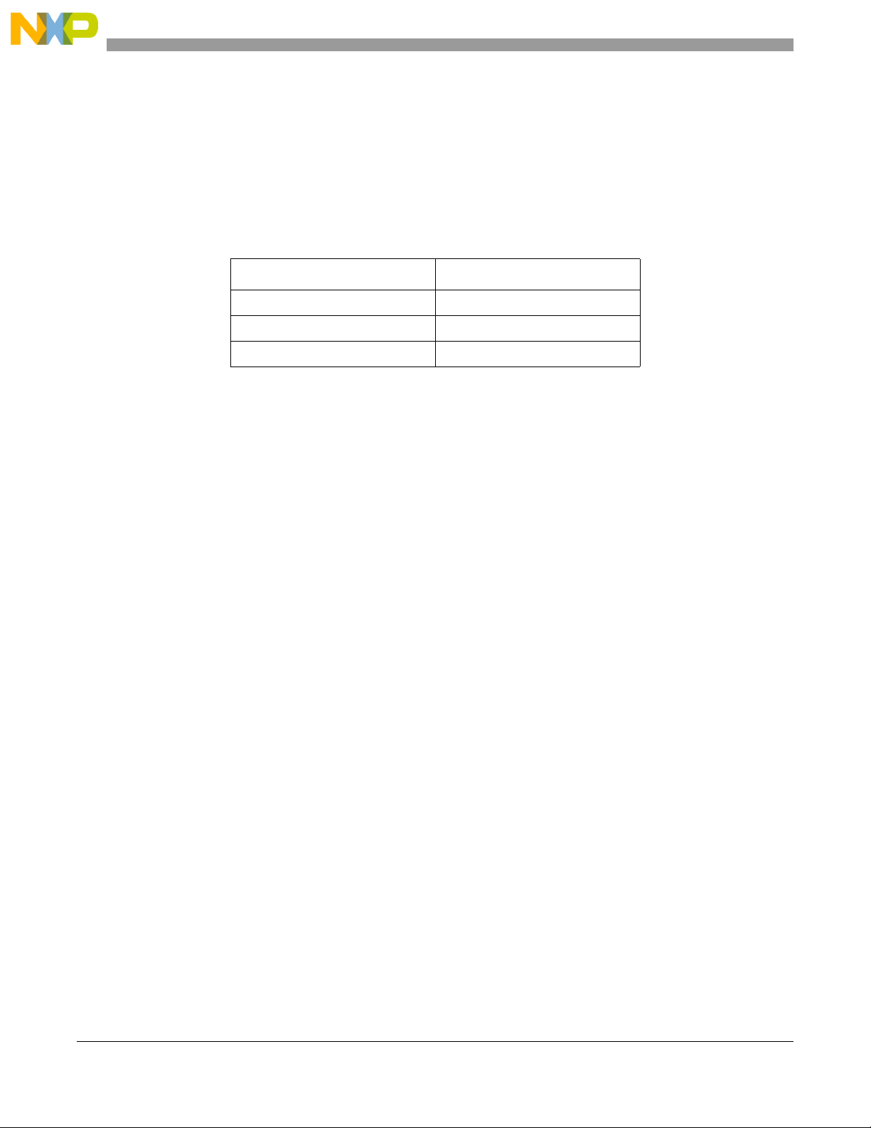
Table 1 shows an example using SDRAM that has 4096 rows and 256 columns, and therefore requires 12
row address lines and eight column address lines. BS[1:0] are connected to A[20:21]
MPC
.
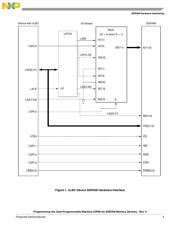
1.2 Address Multiplexing and Bank Select
An SDRAM memory device requires a mixed addressing method. Because of the way the row and column
addresses are multiplexed, during an
ACTIVATE command the row address is driven on the address bus,
and during the READ/WRITE command the column address is driven on the address bus. However, the bank
address is not multiplexed and is driven on BS[1:0] (for a four-bank device) regardless of the current
command. The UPM on the eLBC cannot support this method of operation and can drive either a linear or
a multiplexed address. It cannot use some of the address line in a linear mode (as required for bank address)
and some in a multiplexed mode (as required for row/column address). Glue logic on a host board can
solve this problem.
In the suggested solution, the UPM is programmed to drive the linear address on LAD[0:31] signals of the
device by programming the AMX field to 0b00 in all UPM RAM words. The row and column addresses
are multiplexed on the board using a multiplexer. A control signal must be driven to control the mux.
Because only the user can know that the glue logic exists, a general purpose line to control the mux should
be implemented. LGPL5 can be used to control the address multiplexing on the board because it is unused
in the UPM command patterns for the SDRAM memory device. 2 bits of LAD[0:31] are used as bank
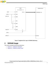
select lines and are not multiplexed. Refer to Figure 2 for a description of glue logic.
NOTE
The suggested solution is relevant only to an SDRAM memory device with
12 row address bits, 8 column address bits, and 4 banks. Adjustments must
be made for devices with a different size or addressing.
Table 1. SDRAM Addressing Example
Device with eLBC SDRAM
A[8:19] 12 bits to cover 4096 rows
A[20:21] BS[1:0]
A[22:29] 8 bits to cover 256 columns
器件 Datasheet 文档搜索
AiEMA 数据库涵盖高达 72,405,303 个元件的数据手册,每天更新 5,000 多个 PDF 文件
