Datasheet 搜索 > 接口芯片 > TI(德州仪器) > P82B715D 数据手册 > P82B715D 用户编程技术手册 2/84 页

 器件3D模型
¥ 9.468
P82B715D 用户编程技术手册 - TI(德州仪器)
制造商:
TI(德州仪器)
分类:
接口芯片
封装:
SOIC-8
描述:
TEXAS INSTRUMENTS P82B715D 专用接口, 4.5 V, 12 V, 8 引脚
Pictures:
3D模型
符号图
焊盘图
引脚图
产品图
页面导航:
导航目录
P82B715D数据手册
Page:
of 84 Go
若手册格式错乱,请下载阅览PDF原文件
TLC271, TLC271A, TLC271B
LinCMOS PROGRAMMABLE LOW-POWER
OPERATIONAL AMPLIFIERS
SLOS090D – NOVEMBER 1987 – REVISED MARCH 2001
2
POST OFFICE BOX 655303 • DALLAS, TEXAS 75265
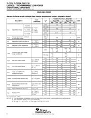
DEVICE FEATURES
PARAMETER
†
BIAS-SELECT MODE
UNIT
PARAMETER
†
HIGH MEDIUM LOW
UNIT
P
D
3375 525 50 µW
SR 3.6 0.4 0.03 V/µs
V
n
25 32 68 nV/√Hz
B
1
1.7 0.5 0.09 MHz
A
VD
23 170 480 V/mV
†
Typical at V
DD
= 5 V, T
A
= 25°C
description (continued)
Using the bias-select option, these cost-effective devices can be programmed to span a wide range of
applications that previously required BiFET, NFET, or bipolar technology. Three offset voltage grades are
available (C-suffix and I-suffix types), ranging from the low-cost TLC271 (10 mV) to the TLC271B (2 mV)
low-offset version. The extremely high input impedance and low bias currents, in conjunction with good
common-mode rejection and supply voltage rejection, make these devices a good choice for new
state-of-the-art designs as well as for upgrading existing designs.
In general, many features associated with bipolar technology are available in LinCMOS operational amplifiers,
without the power penalties of bipolar technology. General applications such as transducer interfacing, analog
calculations, amplifier blocks, active filters, and signal buffering are all easily designed with the TLC271. The
devices also exhibit low-voltage single-supply operation, making them ideally suited for remote and
inaccessible battery-powered applications. The common-mode input voltage range includes the negative rail.
A wide range of packaging options is available, including small-outline and chip-carrier versions for high-density
system applications.
The device inputs and output are designed to withstand –100-mA surge currents without sustaining latch-up.
The TLC271 incorporates internal ESD-protection circuits that prevent functional failures at voltages up to 2000
V as tested under MIL-STD-883C, Method 3015.2; however, care should be exercised in handling these devices
as exposure to ESD may result in the degradation of the device parametric performance.
The C-suffix devices are characterized for operation from 0°C to 70°C. The I-suffix devices are characterized
for operation from –40°C to 85°C. The M-suffix devices are characterized for operation over the full military
temperature range of –55°C to 125°C.
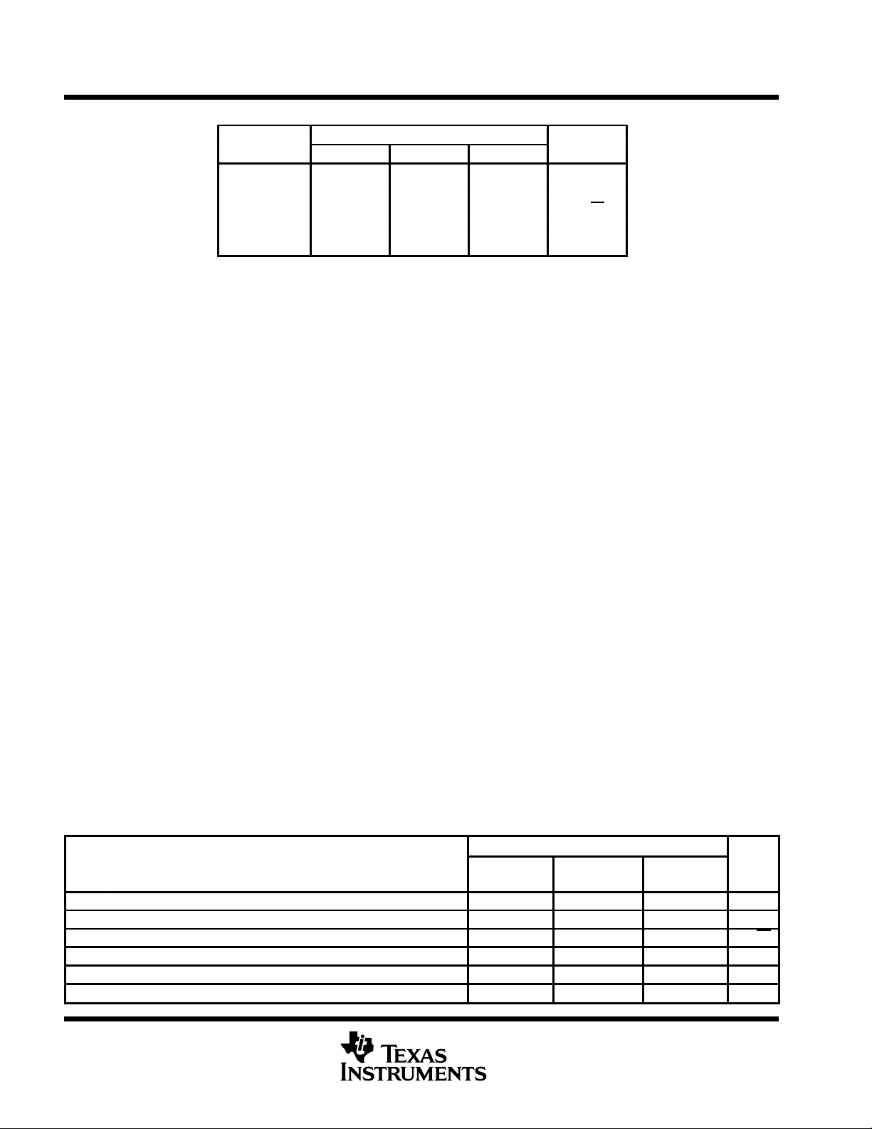
bias-select feature
The TLC271 offers a bias-select feature that allows the user to select any one of three bias levels depending
on the level of performance desired. The tradeoffs between bias levels involve ac performance and power
dissipation (see Table 1).
Table 1. Effect of Bias Selection on Performance
TYPICAL PARAMETER VALUES
MODE
TYPICAL
PARAMETER
VALUES
T
A
=
25
°
C, V
DD
=
5V
HIGH BIAS MEDIUM BIAS LOW BIAS
UNIT
T
A
=
25 C
,
V
DD
=
5
V
R
L
= 10 kΩ R
L
= 100 kΩ R
L
= 1 MΩ
P
D
Power dissipation 3.4 0.5 0.05 mW
SR Slew rate 3.6 0.4 0.03 V/µs
V
n
Equivalent input noise voltage at f = 1 kHz 25 32 68 nV/√Hz
B
1
Unity-gain bandwidth 1.7 0.5 0.09 MHz
φ
m
Phase margin 46° 40° 34°
A
VD
Large-signal differential voltage amplification 23 170 480 V/mV
器件 Datasheet 文档搜索
AiEMA 数据库涵盖高达 72,405,303 个元件的数据手册,每天更新 5,000 多个 PDF 文件
