Datasheet 搜索 > 微控制器 > Microchip(微芯) > PIC10F202-E/MC 数据手册 > PIC10F202-E/MC 用户编程技术手册 4/22 页
 器件3D模型
¥ 4.217
PIC10F202-E/MC 用户编程技术手册 - Microchip(微芯)
制造商:
Microchip(微芯)
分类:
微控制器
封装:
DFN-8
描述:
6引脚8位闪存微控制器 6-Pin, 8-Bit Flash Microcontrollers
Pictures:
3D模型
符号图
焊盘图
引脚图
产品图
页面导航:
引脚图在P1Hot
电气规格在P18

导航目录
PIC10F202-E/MC数据手册
Page:
of 22 Go
若手册格式错乱,请下载阅览PDF原文件
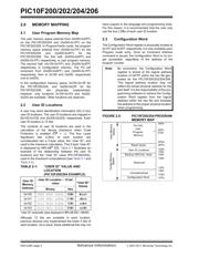
PIC10F200/202/204/206
DS41228F-page 4 Advance Information 2007-2011 Microchip Technology Inc.
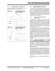
3.0 PROGRAM/VERIFY MODE
In Program/Verify mode, the program memory and the
configuration memory can be accessed and
programmed in serial fashion. ICSPDAT and ICSPCLK
are used for the data and the clock, respectively. All
commands and data words are transmitted LSb first.
Data changes on the rising edge of the ICSPCLK and
is latched on the falling edge. In Program/Verify mode,
both the ICSPDAT and ICSPCLK are Schmitt Trigger
inputs. The sequence that enters the device into
Program/Verify mode places all other logic into the
Reset state. Upon entering Program/Verify mode, all
I/Os are automatically configured as high-impedance
inputs and the address is cleared.
3.1 High-Voltage Program/Verify mode
Entry and Exit
There are two different methods of entering Program/
Verify mode via high-voltage:
•V
DD- First Entry mode
•V
PP- First Entry mode
3.1.1 VPP- FIRST ENTRY MODE
To enter Program/Verify mode via the VPP- first
method, please follow the sequence below:
1. Hold ICSPCLK and ICSPDAT low. All other pins
should be un-powered.
2. Raise the voltage on MCLR
/VPP from 0V to
V
IHH.
3. Raise the voltage on VDD from 0V to the desired
operating voltage.
The V
PP- first entry prevents the device from executing
code prior to entering Program/Verify mode. For
example, when Configuration Word 1 has MCLR
disabled (MCLRE = 0), the power-up time is disabled
(PWRTE = 0), the internal oscillator is selected
(FOSC = 100), and ICSPCLK and ICSPDAT pins are
driven by the user application, the device will execute
code. Since this may prevent entry, VPP- First Entry
mode is strongly recommended. See the timing
diagram in Figure 3-1.
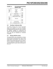
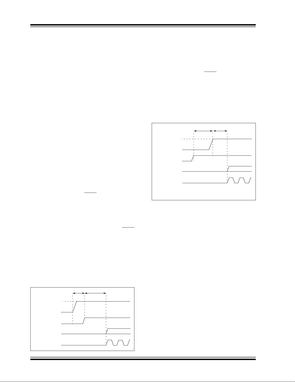
FIGURE 3-1: PROGRAMMING MODE
ENTRY – V
PP FIRST
3.1.2 V
DD- FIRST ENTRY MODE
To enter Program/verify mode via the VDD- first
method, please follow the sequence below:
1. Hold ICSPCLK and ICSPDAT low.
2. Raise the voltage on V
DD from 0V to the desired
operating voltage (V
IL to VDD).
3. Raise the voltage on MCLR/VPP from VDD or
below, to V
IHH.
The V
DD- first method is useful when programming the
device when V
DD is already applied, for it is not
necessary to disconnect V
DD to enter Program/Verify
mode. See the timing diagram in Figure 3-2.
FIGURE 3-2: PROGRAMMING MODE
ENTRY – V
DD FIRST
THLD0
ICSPDAT
ICSPCLK
VDD
TPPDP
VPP
VIHH
VIL
VPP
THLD0
VDD
TPPDP
ICSPDAT
ICSPCLK
VIHH
VIL
器件 Datasheet 文档搜索
AiEMA 数据库涵盖高达 72,405,303 个元件的数据手册,每天更新 5,000 多个 PDF 文件
