Datasheet 搜索 > 微控制器 > Microchip(微芯) > PIC10F204T-I/MC 数据手册 > PIC10F204T-I/MC 用户编程技术手册 2/22 页
 器件3D模型
¥ 1.575
PIC10F204T-I/MC 用户编程技术手册 - Microchip(微芯)
制造商:
Microchip(微芯)
分类:
微控制器
封装:
DFN-8
描述:
6引脚8位闪存微控制器 6-Pin, 8-Bit Flash Microcontrollers
Pictures:
3D模型
符号图
焊盘图
引脚图
产品图
页面导航:
引脚图在P1Hot
电气规格在P18

导航目录
PIC10F204T-I/MC数据手册
Page:
of 22 Go
若手册格式错乱,请下载阅览PDF原文件
PIC10F200/202/204/206
DS41228F-page 2 Advance Information 2007-2011 Microchip Technology Inc.
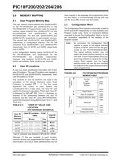
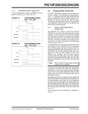
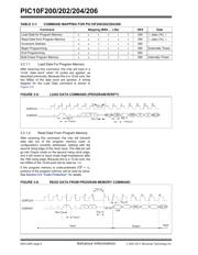
2.0 MEMORY MAPPING
2.1 User Program Memory Map
The user memory space extends from (0x000-0x0FF)
on the PIC10F200/204 and (0x000-0x1FF) on the
PIC10F202/206. In Program/Verify mode, the program
memory space extends from (0x000-0x1FF) for the
PIC10F200/204 and (0x000-0x3FF) for the
PIC10F202/206. The first half, (0x000-0x0FF) and
(0x000-0x1FF) respectively, is user program memory.
The second half, (0x100-0x1FF) and (0x200-0x3FF)
respectively, is configuration memory. The PC will
increment from (0x000-0x0FF) and (0x000-0x1FF)
respectively, then to 0x100 and 0x200, respectively
(not to 0x000).
In the configuration memory space, 0x100-0x13F for
the PIC10F200/204, and 0x200-0x23F for the
PIC10F202/206, are physically implemented.
However, only locations 0x100-0x103 and 0x200-
0x203 are available. Other locations are reserved.
2.2 User ID Locations
A user may store identification information (ID) in four
user ID locations. The user ID locations are mapped in
[0x100:0x103] and [0x200:0x203], respectively. Each
user ID location is 12 bits.
The contents of user ID locations are used in the
calculation of the device checksum when Code
Protection is enabled (CP
= 0). The four Least
Significant bits (LSbs) of each location are
concatenated into a 2-byte value, the “User ID”, and
used in the checksum calculation. This 2-byte “User ID”
is displayed by MPLAB
®
IDE. Table 2-1 illustrates an
example of the relationship between the user ID
locations and the “User ID” value (PIC10F200/204),
used in the checksum computations (see Table 5-1 and
Table 5-2).
Although 12 bits are available in each location,
previous devices only implemented the lower 4 bits of
each location. As a result, these additional bits may not
have support in the language and programming tools.
For this reason, it is recommended that the user only
use the four LSBs of each user ID location.
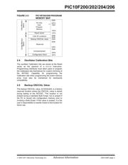
2.3 Configuration Word
The Configuration Word register is physically located at
0x1FF and 0x3FF, respectively. It is only available upon
Program mode entry. Once an Increment Address
command is issued, the Configuration Word is no lon-
ger accessible, regardless of the address of the
program counter.
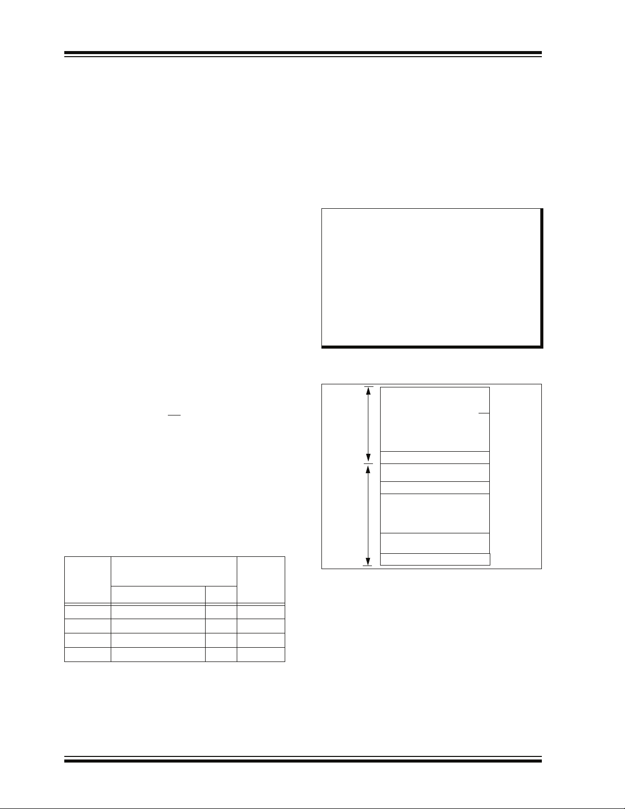
FIGURE 2-2: PIC10F200/204 PROGRAM
MEMORY MAP
TABLE 2-1: “USER ID” VALUE AND
LOCATION
(PIC10F200/204 EXAMPLE)
User ID
Memory
Address
User ID Location – 12-bit
value
“User ID”
Values
Binary Hex
0x100 0000 0000 1001b 009h 9xxxh
0x101 1100 0001 1000b C18hx8xxh
0x102 0111 0010 0100b 724hxx4xh
0x103 0110 0011 0101b 635h xxx5h
“User ID” composite value displayed in MPLAB IDE =
9845h
Note: By convention, the Configuration Word
register is stored at the logical address
location of 0xFFF within the hex file gen-
erated for the PIC10F200/202/204/206.
This logical address location may not
reflect the actual physical address for the
part itself. It is the responsibility of the pro-
gramming software to retrieve the Config-
uration Word register from the logical
address within the hex file and translate
the address to the proper physical location
when programming.
User Memory
Space
000h
Reset Vector
0FFh
On-chip
User
Program
Memory
User ID Locations
Reserved
Configuration Word
100h
-
103h
104h
1FEh
1FFh
13Fh
140h
Unimplemented
0FEh
Backup OSCCAL value
105h
Config Memory
Space
00Fh
010h
器件 Datasheet 文档搜索
AiEMA 数据库涵盖高达 72,405,303 个元件的数据手册,每天更新 5,000 多个 PDF 文件
