Datasheet 搜索 > 微控制器 > Microchip(微芯) > PIC12F509T-I/MC 数据手册 > PIC12F509T-I/MC 用户编程技术手册 1/20 页
 器件3D模型
¥ 7.355
PIC12F509T-I/MC 用户编程技术手册 - Microchip(微芯)
制造商:
Microchip(微芯)
分类:
微控制器
封装:
DFN-8
描述:
8位微控制器 -MCU 1.5KB 41B RAM 4MHz
Pictures:
3D模型
符号图
焊盘图
引脚图
产品图
页面导航:
引脚图在P1Hot
电气规格在P17
导航目录
PIC12F509T-I/MC数据手册
Page:
of 20 Go
若手册格式错乱,请下载阅览PDF原文件
© 2007 Microchip Technology Inc. Preliminary DS41227E-page 1
PIC12F508/509
This document includes the
programming specifications for the
following devices:
•PIC12F508
•PIC12F509
1.0 PROGRAMMING THE
PIC12F508/509
The PIC12F508/509 is programmed using a serial
method. The Serial mode will allow the PIC12F508/509
to be programmed while in the user’s system. This
allows for increased design flexibility. This
programming specification applies to PIC12F508/509
devices in all packages.
1.1 Hardware Requirements
The PIC12F508/509 requires one power supply for
V
DD (5.0V) and one for VPP (12V).
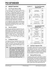
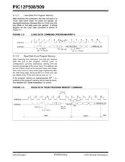
1.2 Program/Verify Mode
The Program/Verify mode for the PIC12F508/509
allows programming of user program memory, user ID
locations, backup OSCCAL location and the Configura-
tion Word.
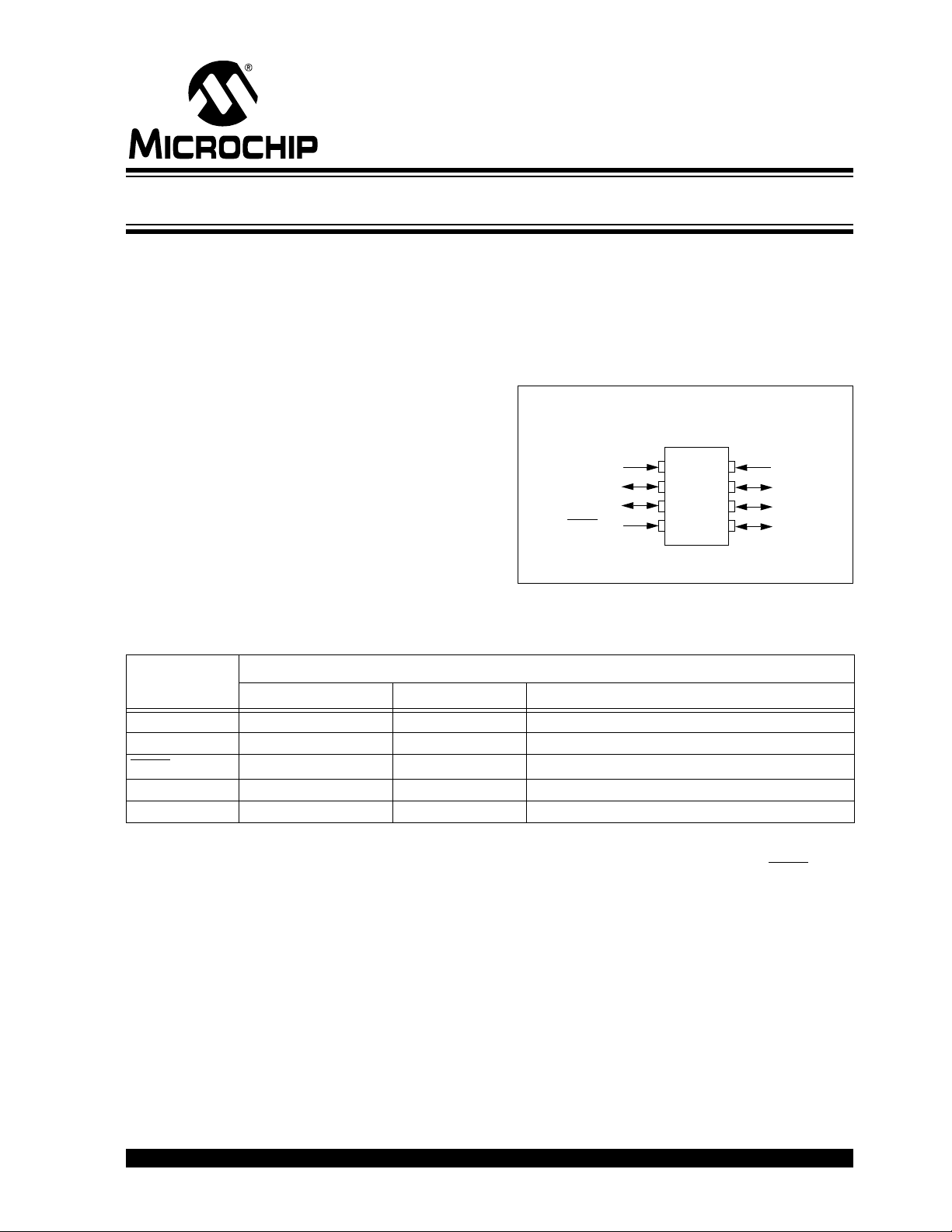
Pin Diagrams
TABLE 1-1: PIN DESCRIPTIONS (DURING PROGRAMMING): PIC12F508/509
PDIP, SOIC, MSOP
VDD
GP5/OSC1/CLKIN
GP4/OSC2
GP3/MCLR
/VPP
1
2
3
4
VSS
GP0/ICSPDAT
8
7
6
5
PIC12F508/509
GP1/ICSPCLK
GP2/T0CKI
Pin Name
During Programming
Function Pin Type Pin Description
GP1 ICSPCLK I Clock input – Schmitt Trigger input
GP0 ICSPDAT I/O Data input/output – Schmitt Trigger input
MCLR
/VPP Program/Verify mode P
(1)
Programming Power
V
DD VDD P Power Supply
VSS VSS P Ground
Legend: I = Input, O = Output, P = Power
Note 1: In the PIC12F508/509, the programming high voltage is internally generated. To activate the Program/
Verify mode, high voltage of I
IHH current capability (see Table 6-1) needs to be applied to the MCLR input.
Memory Programming Specification
器件 Datasheet 文档搜索
AiEMA 数据库涵盖高达 72,405,303 个元件的数据手册,每天更新 5,000 多个 PDF 文件
