Datasheet 搜索 > 微控制器 > Microchip(微芯) > PIC16C505-04/P 数据手册 > PIC16C505-04/P 用户编程技术手册 2/14 页
 器件3D模型
¥ 17.979
PIC16C505-04/P 用户编程技术手册 - Microchip(微芯)
制造商:
Microchip(微芯)
分类:
微控制器
封装:
PDIP-14
描述:
MICROCHIP PIC16C505-04/P 微控制器, 8位, 一次性可编程, PIC16C5xx, 4 MHz, 1.5 KB, 72 Byte, 14 引脚, DIP
Pictures:
3D模型
符号图
焊盘图
引脚图
产品图
页面导航:
引脚图在P1Hot
电气规格在P10
导航目录
PIC16C505-04/P数据手册
Page:
of 14 Go
若手册格式错乱,请下载阅览PDF原文件

PIC16C50X
DS30603B-page 2 2001 Microchip Technology Inc.
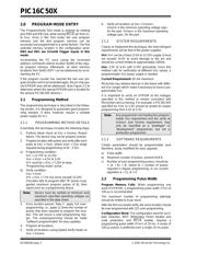
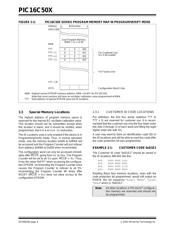
2.0 PROGRAM MODE ENTRY
The Program/Verify Test mode is entered by holding
pins RB0 and RB1 low, while raising MCLR
pin from VIL
to VIHH. Once in this Test mode, the user program
memory and the test program memory can be
accessed and programmed in a serial fashion. The first
selected memory location is the configuration word.
RB0 and RB1 are Schmitt Trigger inputs in this
mode.
Incrementing the PC once (using the increment
address command) selects location 0x000 of the regu-
lar program memory. Afterwards, all other memory
locations from 0x001-03FF can be addressed by incre-
menting the PC.
If the program counter has reached the last user pro-
gram location and is incremented again, the on-chip spe-
cial EPROM area will be addressed. (See Figure 2-2 to
determine where the special EPROM area is located for
the various PIC16C50X devices.)
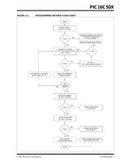
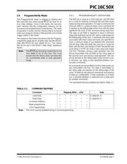
2.1 Programming Method
The programming technique is described in the follow-
ing section. It is designed to guarantee good program-
ming margins. It does, however, require a variable
power supply for V
CC.
2.1.1 PROGRAMMING METHOD DETAILS
Essentially, this technique includes the following steps:
1. Perform blank check at V
DD = VDDMIN. Report
failure. The device may not be properly erased.
2. Program location with pulses and verify after each
pulse at V
DD = VDDP: where VDDP = VDD range
required during programming (4.5V - 5.5V).
a) Programming condition:
V
PP = 12.75V to 13.25V
V
DD = VDDP = 4.5V to 5.5V
V
PP must be ≥ VDD + 7.25V to keep
“Programming mode” active.
b) Verify condition:
V
DD = VDDP
VPP ≥ VDD + 7.5V but not to exceed 13.25V
If location fails to program after “N” pulses (sug-
gested maximum program pulses of 8), then
report error as a programming failure.
3. Once location passes ‘Step 2’, apply 11X over-
programming, i.e., apply 11 times the number of
pulses that were required to program the loca-
tion. This will insure a solid programming mar-
gin. The overprogramming should be made
“software programmable” for easy updates.
4. Program all locations.
5. Verify all locations (using Speed Verify mode) at
V
DD = VDDMIN.
6. Verify all locations at VDD = VDDMAX.
V
DDMIN is the minimum operating voltage spec.
for the part. V
DDMAX is the maximum operating
voltage spec. for the part.
2.1.2 SYSTEM REQUIREMENTS
Clearly, to implement this technique, the most stringent
requirements will be that of the power supplies:
V
PP: VPP can be a fixed 13.0V to 13.25V supply. It must
not exceed 14.0V to avoid damage to the pin and
should be current limited to approximately 100mA.
V
DD: 2.0V to 6.5V with 0.25V granularity. Since this
method calls for verification at different V
DD values, a
programmable V
DD power supply is needed.
Current Requirement: 40 mA maximum
Microchip may release devices in the future with differ-
ent V
DD ranges which make it necessary to have a pro-
grammable V
DD.
It is important to verify an EPROM at the voltages
specified in this method to remain consistent with
Microchip's test screening. For example, a PIC16C50X
specified for 4.5V to 5.5V should be tested for proper
programming from 4.5V to 5.5V.
2.1.3 SOFTWARE REQUIREMENTS
Certain parameters should be programmable (and
therefore, easily modified) for easy upgrade.
a) Pulse width.
b) Maximum number of pulses, present limit 8.
c) Number of over-programming pulses: should be
= (A • N) + B, where N = number of pulses
required in regular programming. In our current
algorithm A = 11, B = 0.
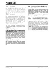
2.2 Programming Pulse Width
Program Memory Cells: When programming one
word of EPROM, a programming pulse width (T
PW) of
100 µs is recommended.
The maximum number of programming attempts
should be limited to 8 per word.
After the first successful verify, the same location should
be over-programmed with 11X over-programming.
Configuration Word: The configuration word for oscil-
lator selection, WDT (Watchdog Timer) disable and
code protection, and MCLR
enable, requires a
programming pulse width (T
PWF) of 10 ms. A series of
100 µs pulses is preferred over a single 10 ms pulse.
Note: Device must be verified at minimum and
maximum specified operating voltages as
specified in the data sheet.
Note: Any programmer not meeting the program-
mable V
DD requirement and the verify at
V
DDMAX and VDDMIN requirement, may
only be classified as a “prototype” or
“development” programmer, but not a
production programmer.
器件 Datasheet 文档搜索
AiEMA 数据库涵盖高达 72,405,303 个元件的数据手册,每天更新 5,000 多个 PDF 文件
