Datasheet 搜索 > 8位微控制器 > Microchip(微芯) > PIC16C558-04I/P 数据手册 > PIC16C558-04I/P 用户编程技术手册 5/16 页
 器件3D模型
¥ 42.779
PIC16C558-04I/P 用户编程技术手册 - Microchip(微芯)
制造商:
Microchip(微芯)
分类:
8位微控制器
封装:
PDIP-18
描述:
PIC16 系列 128 B RAM 2 K x 14位 EPROM 8位 CMOS 微控制器 - PDIP-18
Pictures:
3D模型
符号图
焊盘图
引脚图
产品图
页面导航:
引脚图在P1P2Hot
电气规格在P12
导航目录
PIC16C558-04I/P数据手册
Page:
of 16 Go
若手册格式错乱,请下载阅览PDF原文件
2002 Microchip Technology Inc. DS30261D-page 5
PIC16C55X
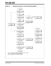
2.2 Program/Verify Mode
The Program/Verify mode is entered by holding pins
RB6 and RB7 low while raising MCLR
pin from VIL to
V
IHH (high voltage). Once in this mode the user pro-
gram memory and the configuration memory can be
accessed and programmed in a serial fashion. The
mode of operation is serial, and the memory that is
accessed is the user program and configuration mem-
ory. RB6 is a Schmitt Trigger input in this mode.
The sequence that enters the device into the Program-
ming/Verify mode places all other logic into the RESET
state (the MCLR
pin was initially at VIL). This means
that all I/O are in the RESET state (High impedance
inputs).
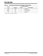
2.2.1 PROGRAM/VERIFY OPERATION
The RB6 pin is used as a clock input pin and the RB7
pin is used for entering command bits and data input/
output during serial operation. To input a command, the
clock pin (RB6) is cycled six times. Each command bit
is latched on the falling edge of the clock with the Least
Significant bit (LSb) of the command being input first.
The data on pin RB7 is required to have a minimum
setup and hold time (see AC/DC specs) with respect to
the falling edge of the clock. Commands that have data
associated with them (Read and Load) are specified to
have a minimum delay of 1 µs between the command
and the data. After this delay the clock pin is cycled 16
times with the first cycle being a START bit and the last
cycle being a STOP bit. Data is also input and output
LSb first. Therefore, during a read operation the LSb
will be transmitted onto pin RB7 on the rising edge of
the second cycle, and during a load operation the LSb
will be latched on the falling edge of the second cycle.
A minimum 1 µs delay is also specified between con-
secutive commands.
The commands that are available are listed in Table 2-
2.
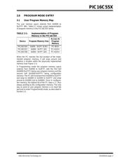
2.2.1.1 Load Configuration
After receiving this command, the program counter
(PC) will be set to 0x2000. By then applying 16 cycles
to the clock pin, the chip will load 14-bits a “data word”
as described above, to be programmed into the config-
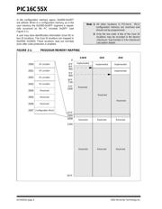
uration memory. A description of the memory mapping
schemes for normal operation and Configuration mode
operation is shown in Figure 2-1. After the configura-
tion memory is entered, the only way to get back to the
user program memory is to exit the Program/Verify Test
mode by taking MCLR
low (VIL).
TABLE 2-2: COMMAND MAPPING
Note: The MCLR pin should be raised as quickly
as possible from V
IL to VIHH. This is to
ensure that the device does not have the
PC incremented while in valid operation
range.
Command Mapping (MSB ... LSB) Data
Load Configuration 000000 0, data(14), 0
Load Data 000010 0, data(14), 0
Read Data 000100 0, data(14), 0
Increment Address 000110
Begin Programming 001000
End Programming 001110
Note: The CPU clock must be disabled during in-circuit programming.
器件 Datasheet 文档搜索
AiEMA 数据库涵盖高达 72,405,303 个元件的数据手册,每天更新 5,000 多个 PDF 文件
