Datasheet 搜索 > 微控制器 > Microchip(微芯) > PIC16F676-I/ML 数据手册 > PIC16F676-I/ML 用户编程技术手册 5/24 页
 器件3D模型
¥ 13.807
PIC16F676-I/ML 用户编程技术手册 - Microchip(微芯)
制造商:
Microchip(微芯)
分类:
微控制器
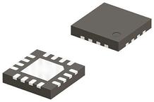
封装:
QFN-16
描述:
PIC16F630/676 8 位闪存微控制器Microchip 的 PIC16F 系列微控制器 8 位 MCU,将 Microchip 的 PIC® 体系架构融入到引脚和封装选件中,从节省空间的 14 引脚设备到功能丰富的 64 引脚设备。 带有基线、中级或增强型中级体系架构的设备提供多种不同的外围设备组合,可谓设计人员提供灵活性,并为应用提供选择。 PIC16F630/676 系列微控制器基于 Microchip 的中级内核,带 8 层深硬件堆栈和 35 个指令。 这些 MCU 提供高达 5 个 MIP、1.75 千字节程序存储器、64 字节 RAM 和 128 字节数据 EEPROM。 板载是一个振荡器,工厂校准到 ±1% 精确度。### 微控制器功能最大 20 MHz CPU 速度 35 指令 8 级硬件堆栈 4 MHz 内部振荡器 12 个输入/输出引脚 通电重置 (POR) 通电计时器 (PWRT) 振荡器启动计时器 (OST) 掉电检测 (BOD) 监控器计时器 (WDT) 在线串行编程 (ICSP) ### 外设8 通道 10 位模拟到数字转换器 – 仅限 PIC16F676 一个比较器 一个 8 位计时器 一个 16 位计时器 ### PIC16 微控制器
Pictures:
3D模型
符号图
焊盘图
引脚图
产品图
页面导航:
引脚图在P1P2P3Hot
电气规格在P21

导航目录
PIC16F676-I/ML数据手册
Page:
of 24 Go
若手册格式错乱,请下载阅览PDF原文件
© 2005 Microchip Technology Inc. DS41191D-page 5
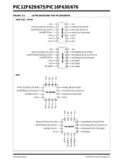
PIC12F629/675/PIC16F630/676
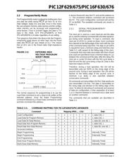
2.3 Program/Verify Mode
The Program/Verify mode is entered by holding pins clock
and data low while raising MCLR
pin from VIL to VIHH
(high voltage). Apply VDD and data. Once in this mode,
the user program memory, data memory and the configu-
ration memory can be accessed and programmed in
serial fashion. Clock is Schmitt Trigger and data is TTL
input in this mode. GP4 (PIC12F629/675) or RA4
(PIC16F630/676) is tri-state, regardless of use setting.
The sequence that enters the device into the Program-
ming/Verify mode places all other logic into the Reset
state (the MCLR
pin was initially at VIL). This means
that all I/O’s are in the Reset state (high-impedance
inputs).
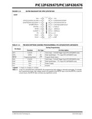
FIGURE 2-2: ENTERING HIGH
VOLTAGE PROGRAM/
VERIFY MODE
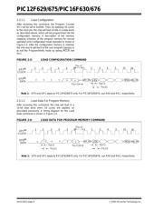
The normal sequence for programming is to use the
Load Data command to set a value to be written at the
selected address. Issue the Begin Programming
command followed by a Read Data command to verify
and then increment the address.
A device Reset will clear the PC and set the address to
‘0’. The Increment Address command will increment
the PC. The Load Configuration command will set the
PC to 0x2000. The available commands are shown in
Table 2-1.
2.3.1 SERIAL PROGRAM/VERIFY
OPERATION
The clock pin is used as a clock input pin and the data
pin is used for entering command bits and data input/out-
put during serial operation. To input a command, the
clock pin (CLOCK) is cycled six times. Each command
bit is latched on the falling edge of the clock with the LSb
of the command being input first. The data on pin DATA
is required to have a minimum setup and hold time (see
Table 5-1), with respect to the falling edge of the clock.
Commands that have data associated with them (Read
and Load) are specified to have a minimum delay of 1 μs
between the command and the data. After this delay, the
clock pin is cycled 16 times with the first cycle being a
Start bit and the last cycle being a Stop bit. Data is also
input and output LSb first.
Therefore, during a read operation, the LSb will be
transmitted onto pin DATA on the rising edge of the
second cycle. During a load operation, the LSb will be
latched on the falling edge of the second cycle. A
minimum 1 μs delay is also specified between
consecutive commands.
All commands are transmitted LSb first. Data words are
also transmitted LSb first. The data is transmitted on
the rising edge and latched on the falling edge of the
clock. To allow for decoding of commands and reversal
of data pin configuration, a time separation of at least
1 μs is required between a command and a data word
(or another command).
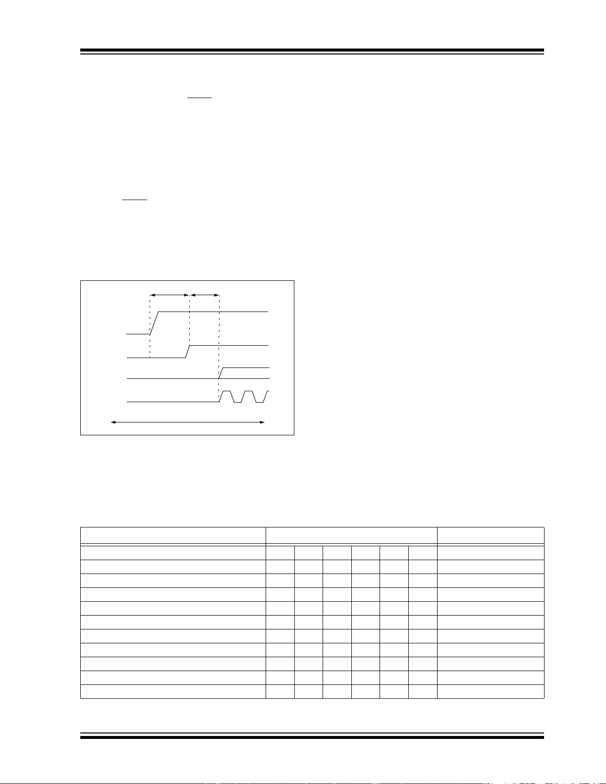
The commands that are available are described in
Table 2-1.
TABLE 2-1: COMMAND MAPPING FOR PIC12F629/675/PIC16F630/676
VPP
THLD0
DATA
SDATA = Input
CLOCK
VDD
TPPDP
Command Mapping (MSb … LSb) Data
Load Configuration XX00000, data (14), 0
Load Data for Program Memory XX00100, data (14), 0
Load Data for Data Memory XX00110, data (8), zero (6), 0
Read Data from Program Memory XX01000, data (14), 0
Read Data from Data Memory XX01010, data (8), zero (6), 0
Increment Address XX0110
Begin Programming 001000Internally Timed
Begin Programming 011000Externally Timed
End Programming 001010
Bulk Erase Program Memory XX1001Internally Timed
Bulk Erase Data Memory XX1011Internally Timed
器件 Datasheet 文档搜索
AiEMA 数据库涵盖高达 72,405,303 个元件的数据手册,每天更新 5,000 多个 PDF 文件
