Datasheet 搜索 > 8位微控制器 > Microchip(微芯) > PIC16F77-I/P 数据手册 > PIC16F77-I/P 用户编程技术手册 1/16 页
 器件3D模型
¥ 47.302
PIC16F77-I/P 用户编程技术手册 - Microchip(微芯)
制造商:
Microchip(微芯)
分类:
8位微控制器
封装:
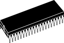
DIP-40
描述:
MICROCHIP PIC16F77-I/P 微控制器, 8位, 闪存, PIC16F, 20 MHz, 14 KB, 368 Byte, 40 引脚, DIP
Pictures:
3D模型
符号图
焊盘图
引脚图
产品图
页面导航:
引脚图在P1Hot
电气规格在P12
导航目录
PIC16F77-I/P数据手册
Page:
of 16 Go
若手册格式错乱,请下载阅览PDF原文件
2002 Microchip Technology Inc. DS30324B-page 1
M
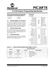
PIC16F7X
This document includes the programming
specifications for the following devices:
1.0 PROGRAMMING THE PIC16F7X
The PIC16F7X is programmed using a serial method.
The Serial mode allows the PIC16F7X to be pro-
grammed while in the users’ system, allowing for
increased design flexibility. This programming specifi-
cation applies to PIC16F7X devices in all packages.
1.1 Hardware Requirements
The PIC16F7X requires two programmable power sup-
plies, one for V
DD (2.0V to 5.5V) and the other for VPP
of 12.75V to 13.25V. Both supplies should have a min-
imum resolution of 0.25V.
1.2 Programming Mode
The Programming mode for the PIC16F7X allows pro-
gramming of user program memory, special locations
used for ID, and the configuration word.
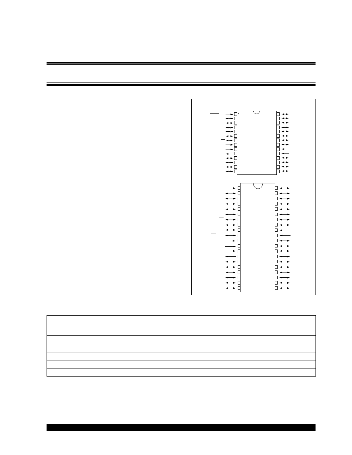
Pin Diagram
• PIC16F73 • PIC16F76
• PIC16F74 • PIC16F77
PDIP, SOIC
RB7PGD
RB6/PGC
RB5
RB4
RB3
RB2
RB1
RB0/INT
V
DD
VSS
RD7/PSP7
RD6/PSP6
RD5/PSP5
RD4/PSP4
RC7/RX/DT
RC6/TX/CK
RC5/SDO
RC4/SDI/SDA
RD3/PSP3
RD2/PSP2
MCLR/VPP
RA0/AN0
RA1/AN1
RA2/AN2
RA3/AN3/VREF
RA4/T0CKI
RA5/AN4/SS
RE0/RD/AN5
RE1/WR/AN6
RE2/CS/AN7
V
DD
VSS
OSC1/CLKIN
OSC2/CLKOUT
RC0/T1OSO/T1CKI
RC1/T1OSI/CCP2
RC2/CCP1
RC3/SCK/SCL
RD0/PSP0
RD1/PSP1
1
2
3
4
5
6
7
8
9
10
11
12
13
14
15
16
17
18
19
20
40
39
38
37
36
35
34
33
32
31
30
29
28
27
26
25
24
23
22
21
PIC16F73/76
10
11
2
3
4
5
6
1
8
7
9
12
13
14
15
16
17
18
19
20
23
24
25
26
27
28
22
21
MCLR/VPP
RA0/AN0
RA1/AN1
RA2/AN2
RA3/AN3/V
REF
RA4/T0CKI
RA5/AN4/SS
VSS
OSC1/CLKIN
OSC2/CLKOUT
RC0/T1OSO/T1CKI
RC1/T1OSI/CCP2
RC2/CCP1
RC3/SCK/SCL
RB7/PGD
RB6/PGC
RB5
RB4
RB3
RB2
RB1
RB0/INT
V
DD
VSS
RC7/RX/DT
RC6/TX/CK
RC5/SDO
RC4/SDI/SDA
PIC16F74/77
TABLE 1-1: PIN DESCRIPTIONS (DURING PROGRAMMING): PIC16F7X
Pin Name
During Programming
Function Pin Type Pin Description
RB6/PGC CLOCK I Clock Input
RB7/PGD DATA I/O Data Input/Output
MCLR
/VPP MODE CONTROL P Program Mode Select
V
DD VDD P Power Supply
VSS VSS P Ground
Legend: I = Input, O = Output, P = Power
FLASH Memory Programming Specification
器件 Datasheet 文档搜索
AiEMA 数据库涵盖高达 72,405,303 个元件的数据手册,每天更新 5,000 多个 PDF 文件
