Datasheet 搜索 > 8位微控制器 > Microchip(微芯) > PIC16F77-I/P 数据手册 > PIC16F77-I/P 用户编程技术手册 4/16 页
 器件3D模型
¥ 47.237
PIC16F77-I/P 用户编程技术手册 - Microchip(微芯)
制造商:
Microchip(微芯)
分类:
8位微控制器
封装:
DIP-40
描述:
MICROCHIP PIC16F77-I/P 微控制器, 8位, 闪存, PIC16F, 20 MHz, 14 KB, 368 Byte, 40 引脚, DIP
Pictures:
3D模型
符号图
焊盘图
引脚图
产品图
页面导航:
引脚图在P1Hot
电气规格在P12
导航目录
PIC16F77-I/P数据手册
Page:
of 16 Go
若手册格式错乱,请下载阅览PDF原文件

PIC16F7X
DS30324B-page 4 2002 Microchip Technology Inc.
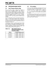
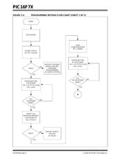
2.3 Program/Verify Mode
The Program/Verify mode is entered by holding pins
RB6 and RB7 low, while raising MCLR
pin from VIL to
V
PP. Once in this mode, the user program memory and
the configuration memory can be accessed and pro-
grammed in serial fashion. (RB6 and RB7 are Schmitt
Trigger Inputs in this mode.)
The sequence that enters the device into the Program-
ming/Verify mode, places all other logic into the RESET
state. All I/O pins are in the RESET state (high imped-
ance inputs).
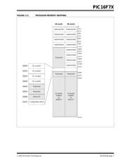
A device RESET will clear the PC and point to address
0x0000. The ‘Increment Address’ command will incre-
ment the PC. The ‘Load Configuration’ command will
set the PC to 0x2000. The available commands are
shown in Table 2-2.
The normal sequence for programming two program
memory words at a time is as follows:
1. Issue the ‘Load Data’ command to load a word
at the current (even) program memory address.
2. Issue an ‘Increment Address’ command.
3. Load a word at the current (odd) program mem-
ory address using the ‘Load Data’ command.
4. Issue a ‘Begin Programming’ command to begin
programming.
5. Wait tprog (about 1 ms).
6. Issue an ‘End Programming’ command.
7. Increment to the next address.
8. Repeat this sequence as required to write pro-
gram and configuration memory.
The alternative sequence for programming one pro-
gram memory word at a time is as follows:
1. Set a word for the current memory location using
the ‘Load Data’ command.
2. Issue a ‘Begin Programming’ command to begin
programming.
3. Wait tprog.
4. Issue an ‘End Programming’ command.
5. Increment to the next address.
6. Repeat this alternative sequence as required to
write program and configuration memory.
The address and program counter is reset to 0x0000 by
resetting the device (taking MCLR
below VIL) and re-
entering Programming mode. Program and configura-
tion memory may then be read or verified using the
Read Data and Increment Address commands.
2.3.1 SERIAL PROGRAM/VERIFY
OPERATION
RB6 is used as a clock input pin, and RB7 is used for
entering command bits and data input/output. To enter
a command, the clock pin (RB6) is pulsed six times.
Each command bit is latched on the falling edge of the
clock (RB6), with the Least Significant bit (LSb) of the
command being input first. The data on pin RB7 needs
a minimum setup (tset1) and hold time (thold1) with
respect to the falling edge of the clock. The read and
load commands are specified to have a minimum delay
(tdly1) between the command and data. After this delay,
the clock pin is cycled 16 times, with the first cycle being
a START bit (0) and the last cycle being a STOP bit (0).
Data is transferred LSb first (see Figure 5-1).
During a read operation, the LSb will be output on pin
RB7 on the rising edge of the second clock pulse and
during a load operation, the LSb will be latched on the
falling edge of the second clock pulse. A minimum
delay (tdly2) is required between consecutive
commands (see Figure 5-2).
To allow for decoding of commands and reversal of
data pin configuration, a time separation of at least
(tdly1) is required between a command and a data
word, or another command (see Figure 5-3).
The available commands are listed below:
• Load Configuration
• Load Data for Memory
• Read Data from Memory
• Increment Address
• Begin Programming
• Bulk Erase Program Memory
• End Programming
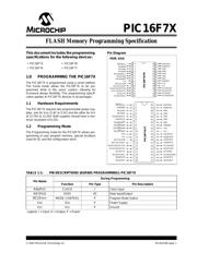
TABLE 2-2: COMMAND MAPPING FOR PIC16F7X
Command Mapping (LSb … MSb) Data (LSb first)
Load Configuration (Set PC = 2000h) 0000XX0, data (14), 0
Load Data for Memory 0100XX0, data (14), 0
Read Data from Memory 0010XX0, data (14), 0
Increment Address 0110XX
Begin Programming 0001XX
Bulk Erase Program Memory (Chip Erase) 1001XX
End Programming 0111XX
器件 Datasheet 文档搜索
AiEMA 数据库涵盖高达 72,405,303 个元件的数据手册,每天更新 5,000 多个 PDF 文件
