Datasheet 搜索 > 微控制器 > Microchip(微芯) > PIC16LF876-04I/SP 数据手册 > PIC16LF876-04I/SP 用户编程技术手册 3/22 页
 器件3D模型
¥ 52.939
PIC16LF876-04I/SP 用户编程技术手册 - Microchip(微芯)
制造商:
Microchip(微芯)
分类:
微控制器
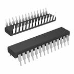
封装:
DIP-28
描述:
PIC16 系列 368 B RAM 14 kB 闪存 8位 CMOS 微控制器 - SDIP-28
Pictures:
3D模型
符号图
焊盘图
引脚图
产品图
页面导航:
引脚图在P2Hot
电气规格在P18

导航目录
PIC16LF876-04I/SP数据手册
Page:
of 22 Go
若手册格式错乱,请下载阅览PDF原文件
2002 Microchip Technology Inc. DS39025F-page 3
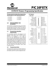
PIC16F87X
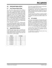
2.0 PROGRAM MODE ENTRY
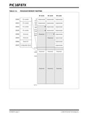
2.1 User Program Memory Map
The user memory space extends from 0x0000 to
0x1FFF (8K). In Programming mode, the program
memory space extends from 0x0000 to 0x3FFF, with
the first half (0x0000-0x1FFF) being user program
memory and the second half (0x2000-0x3FFF) being
configuration memory. The PC will increment from
0x0000 to 0x1FFF and wrap to 0x0000, 0x2000 to
0x3FFF and wrap around to 0x2000 (not to 0x0000).
Once in configuration memory, the highest bit of the PC
stays a ‘1’, thus always pointing to the configuration
memory. The only way to point to user program mem-
ory is to reset the part and re-enter Program/Verify
mode, as described in Section 2.4.
In the configuration memory space, 0x2000-0x200F
are physically implemented. However, only locations
0x2000 through 0x2007 are available. Other locations
are reserved. Locations beyond 0x200F will physically
access user memory (see Figure 2-1).
2.2 Data EEPROM Memory
The EEPROM data memory space is a separate block
of high endurance memory that the user accesses
using a special sequence of instructions. The amount
of data EEPROM memory depends on the device and
is shown below in number of bytes.
The contents of data EEPROM memory have the capa-
bility to be embedded into the HEX file.
The programmer should be able to read data EEPROM
information from a HEX file and conversely (as an
option), write data EEPROM contents to a HEX file,
along with program memory information and configura-
tion bit information.
The 256 data memory locations are logically mapped
starting at address 0x2100. The format for data mem-
ory storage is one data byte per address location, LSB
aligned.
2.3 ID Locations
A user may store identification information (ID) in four
ID locations. The ID locations are mapped in [0x2000 :
0x2003]. It is recommended that the user use only the
four Least Significant bits of each ID location. In some
devices, the ID locations read out in an unscrambled
fashion after code protection is enabled. For these
devices, it is recommended that ID location is written as
“11 1111 1000 bbbb” where ‘bbbb’ is ID information.
In other devices, the ID locations read out normally,
even after code protection. To understand how the
devices behave, refer to Table 5-1.
To understand the scrambling mechanism after code
protection, refer to Section 4.0.
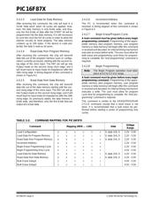
Device # of Bytes
PIC16F870 64
PIC16F871 64
PIC16F872 64
PIC16F873 128
PIC16F874 128
PIC16F876 256
PIC16F877 256
器件 Datasheet 文档搜索
AiEMA 数据库涵盖高达 72,405,303 个元件的数据手册,每天更新 5,000 多个 PDF 文件
