Datasheet 搜索 > 微控制器 > Microchip(微芯) > PIC16LF876-04I/SP 数据手册 > PIC16LF876-04I/SP 用户编程技术手册 6/22 页
 器件3D模型
¥ 52.958
PIC16LF876-04I/SP 用户编程技术手册 - Microchip(微芯)
制造商:
Microchip(微芯)
分类:
微控制器
封装:
DIP-28
描述:
PIC16 系列 368 B RAM 14 kB 闪存 8位 CMOS 微控制器 - SDIP-28
Pictures:
3D模型
符号图
焊盘图
引脚图
产品图
页面导航:
引脚图在P2Hot
电气规格在P18

导航目录
PIC16LF876-04I/SP数据手册
Page:
of 22 Go
若手册格式错乱,请下载阅览PDF原文件

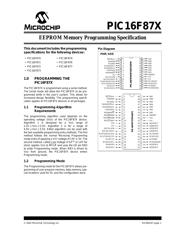
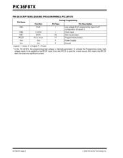
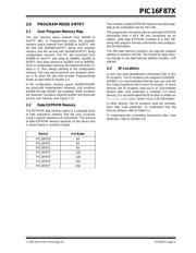
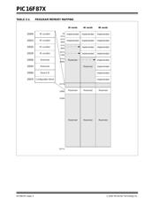
PIC16F87X
DS39025F-page 6 2002 Microchip Technology Inc.
2.4.2.3 Load Data for Data Memory
After receiving this command, the chip will load in a
14-bit “data word” when 16 cycles are applied. How-
ever, the data memory is only 8-bits wide, and thus,
only the first 8-bits of data after the START bit will be
programmed into the data memory. It is still necessary
to cycle the clock the full 16 cycles in order to allow the
internal circuitry to reset properly. The data memory
contains up to 256 bytes. If the device is code pro-
tected, the data is read as all zeros.
2.4.2.4 Read Data from Program Memory
After receiving this command, the chip will transmit
data bits out of the program memory (user or configu-
ration) currently accessed, starting with the second ris-
ing edge of the clock input. The RB7 pin will go into
Output mode on the second rising clock edge, and it
will revert back to Input mode (hi-impedance) after the
16th rising edge. A timing diagram of this command is
shown in Figure 6-2.
2.4.2.5 Read Data from Data Memory
After receiving this command, the chip will transmit
data bits out of the data memory starting with the sec-
ond rising edge of the clock input. The RB7 pin will go
into Output mode on the second rising edge, and it will
revert back to Input mode (hi-impedance) after the 16th
rising edge. As previously stated, the data memory is
8-bits wide, and therefore, only the first 8-bits that are
output are actual data.
2.4.2.6 Increment Address
The PC is incremented when this command is
received. A timing diagram of this command is shown
in Figure 6-3.
2.4.2.7 Begin Erase/Program Cycle
A load command must be given before every begin
programming command. Programming of the appro-
priate memory (test program memory, user program
memory or data memory) will begin after this command
is received and decoded. An internal timing mechanism
executes an erase before write. The user must allow for
both erase and programming cycle times for program-
ming to complete. No “end programming” command is
required.
2.4.2.8 Begin Programming
A load command must be given before every begin
programming command. Programming of the appro-
priate memory (test program memory, user program
memory or data memory) will begin after this command
is received and decoded. An internal timing mechanism
executes a write. The user must allow for program
cycle time for programming to complete. No “end pro-
gramming” command is required.
This command is similar to the ERASE/PROGRAM
CYCLE command, except that a word erase is not
done. It is recommended that a bulk erase be per-
formed before starting a series of programming only
cycles.
Note: The Begin Program operation must take
place at 4.5 to 5.5 V
DD range.
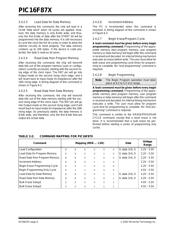
TABLE 2-2: COMMAND MAPPING FOR PIC16F87X
Command Mapping (MSB … LSB) Data
Voltage
Range
Load Configuration XX00000, data (14), 0 2.2V - 5.5V
Load Data for Program Memory XX00100, data (14), 0 2.2V - 5.5V
Read Data from Program Memory XX01000, data (14), 0 2.2V - 5.5V
Increment Address XX0110 2.2V - 5.5V
Begin Erase Programming Cycle 001000 2.2V - 5.5V
Begin Programming Only Cycle 011000 4.5V - 5.5V
Load Data for Data Memory XX00110, data (14), 0 2.2V - 5.5V
Read Data from Data Memory XX01010, data (14), 0 2.2V - 5.5V
Bulk Erase Setup1 000001 4.5V - 5.5V
Bulk Erase Setup2 000111 4.5V - 5.5V
器件 Datasheet 文档搜索
AiEMA 数据库涵盖高达 72,405,303 个元件的数据手册,每天更新 5,000 多个 PDF 文件
