Datasheet 搜索 > 微控制器 > Microchip(微芯) > PIC18F97J60-I/PT 数据手册 > PIC18F97J60-I/PT 用户编程技术手册 5/24 页
 器件3D模型
¥ 25.268
PIC18F97J60-I/PT 用户编程技术手册 - Microchip(微芯)
制造商:
Microchip(微芯)
分类:
微控制器
封装:
TQFP-100
描述:
MICROCHIP PIC18F97J60-I/PT. 芯片, 8位微控制器
Pictures:
3D模型
符号图
焊盘图
引脚图
产品图
页面导航:
引脚图在P1P2P3P4Hot
导航目录
PIC18F97J60-I/PT数据手册
Page:
of 24 Go
若手册格式错乱,请下载阅览PDF原文件
© 2009 Microchip Technology Inc. DS39688D-page 5
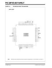
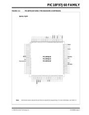
PIC18F97J60 FAMILY
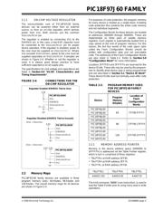
2.1.1 ON-CHIP VOLTAGE REGULATOR
The microcontroller core of PIC18F97J60 family
devices can be powered either from an external
source, or from an on-chip regulator, which derives
power from V
DD. Both sources use the common
VDDCORE/VCAP pin.
The regulator is enabled by connecting V
DD to the
ENVREG pin. In this case, a low-ESR capacitor must
be connected to the VDDCORE/VCAP pin for proper
device operation. If the regulator is disabled, power to
the core must be supplied on V
DDCORE/VCAP. Where
V
DD exceeds VDDCOREMAX, power to the core must be
supplied separately on VDDCORE/VCAP. Examples are
shown in Figure 2-4. Whether or not the regulator is
used, it is always good design practice to have
sufficient capacitance on all supply pins.
The specifications for core voltage and capacitance are
listed in Section 6.0 “AC/DC Characteristics and
Timing Requirements”.
FIGURE 2-4: CONNECTIONS FOR THE
ON-CHIP REGULATOR
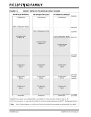
2.2 Memory Maps
PIC18F97J60 family devices are available in three
program memory sizes: 64 Kbytes, 96 Kbytes and
128 Kbytes. The overall memory maps for all devices
are shown in Figure 2-5.
For purposes of code protection, the program memory
for every device is treated as a single block. Enabling
code protection thus protects the entire code memory
and not individual segments.
The Configuration Words for these devices are located
at addresses 300000h through 300005h. These are
implemented as three pairs of volatile memory
registers. Each register is automatically loaded from a
copy stored at the end of program memory. For this
reason, the last four words of the code space (also
called the Flash Configuration Words) should be
written with configuration data and not executable
code. The addresses of the Flash Configuration Words
are also listed in Table 2-2. Refer to Section 5.0
“Configuration Word” for more information.
Locations 3FFFFEh and 3FFFFFh are reserved for the
device ID bits. These bits may be used by the program-
mer to identify what device type is being programmed
and are described in Section 5.1 “Device ID Word”.
These device ID bits read out normally, even after code
protection.
TABLE 2-2: PROGRAM MEMORY SIZES
FOR PIC18F97J60 FAMILY
DEVICES
2.2.1 MEMORY ADDRESS POINTER
Memory in the device address space (000000h to
3FFFFFh) is addressed via the Table Pointer register,
which in turn is comprised of three registers:
• TBLPTRU at RAM address 0FF8h
• TBLPTRH at RAM address 0FF7h
• TBLPTRL at RAM address 0FF6h
The 4-bit command, ‘0000’ (core instruction), is used to
load the Table Pointer prior to using many read or write
operations.
2.5V
VDD
VDDCORE/VCAP
VSS
CF
3.3V
Regulator Enabled (ENVREG Tied to VDD):
Regulator Disabled (ENVREG Tied to Ground):
2.5V 3.3V
(V
DD = VDDCORE)
(V
DD > VDDCORE)
ENVREG
PIC18FXXJ60/65
V
DD
VDDCORE/VCAP
VSS
ENVREG
PIC18FXXJ60/65
V
DD
VDDCORE/VCAP
VSS
ENVREG
PIC18FXXJ60/65
Device
Program
Memory
(Kbytes)
Location of
Flash
Configuration
Words
PIC18F66J60
64 FFF8h:FFFFh
PIC18F86J60
PIC18F96J60
PIC18F66J65
96 17FF8h:17FFFhPIC18F86J65
PIC18F96J65
PIC18F67J60
128 1FFF8h:1FFFFhPIC18F87J60
PIC18F97J60
TBLPTRU TBLPTRH TBLPTRL
Addr[21:16] Addr[15:8] Addr[7:0]
器件 Datasheet 文档搜索
AiEMA 数据库涵盖高达 72,405,303 个元件的数据手册,每天更新 5,000 多个 PDF 文件
