Datasheet 搜索 > 开发套件 > TI(德州仪器) > TPS74901EVM-210 数据手册 > TPS74901EVM-210 用户编程技术手册 4/33 页

¥ 86.189
TPS74901EVM-210 用户编程技术手册 - TI(德州仪器)
制造商:
TI(德州仪器)
分类:
开发套件
描述:
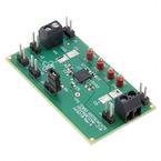
TEXAS INSTRUMENTS TPS74901EVM-210 评估板, TPS74901 可调 3A 稳压器
Pictures:
3D模型
符号图
焊盘图
引脚图
产品图
页面导航:
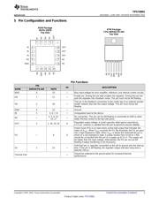
引脚图在P3Hot
典型应用电路图在P1P15P18
原理图在P11P15P20
封装尺寸在P25P27P28
标记信息在P25P26
封装信息在P24P25P26P27P28
技术参数、封装参数在P4
应用领域在P1P33
电气规格在P6
导航目录
TPS74901EVM-210数据手册
Page:
of 33 Go
若手册格式错乱,请下载阅览PDF原文件
TPS74901
SBVS082H –JUNE 2007–REVISED NOVEMBER 2015
www.ti.com
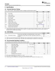
6 Specifications
6.1 Absolute Maximum Ratings
At T
J
= –40°C to 125° C, unless otherwise noted. All voltages are with respect to GND.
(1)
MIN MAX UNIT
V
IN
,
Input voltage –0.3 6 V
V
BIAS
V
EN
Enable voltage –0.3 6 V
V
PG
Power-good voltage –0.3 6 V
I
PG
PG sink current 0 1.5 mA
V
SS
SS pin voltage –0.3 6 V
V
FB
Feedback pin voltage –0.3 6 V
V
OUT
Output voltage –0.3 V
IN
+ 0.3 V
I
OUT
Maximum output current Internally limited
Output short circuit duration Indefinite
P
DISS
Continuous total power dissipation See Thermal Information
T
J
Operating junction temperature –40 125 °C
T
stg
Storage junction temperature –55 150 °C
(1) Stresses beyond those listed under Absolute Maximum Ratings may cause permanent damage to the device. These are stress ratings
only and functional operation of the device at these conditions is not implied. Exposure to absolute-maximum-rated conditions for
extended periods may affect device reliability.
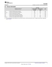
6.2 ESD Ratings
VALUE UNIT
Human body model (HBM), per ANSI/ESDA/JEDEC JS-001, all pins
(1)
±2000
V
(ESD)
Electrostatic discharge V
Charged device model (CDM), per JEDEC specification JESD22-C101,
±500
all pins
(2)
(1) JEDEC document JEP155 states that 500-V HBM allows safe manufacturing with a standard ESD control process.
(2) JEDEC document JEP157 states that 250-V CDM allows safe manufacturing with a standard ESD control process.
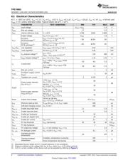
6.3 Recommended Operating Conditions
over operating junction temperature range (unless otherwise noted)
MIN NOM MAX UNIT
V
IN
Input supply voltage V
OUT
+ V
DO
(V
IN
) 5.5 V
V
EN
Enable supply voltage 0 5.5 V
V
BIAS
(1)
BIAS supply voltage V
OUT
+ V
DO
(V
BIAS
)
(2)
5.5 V
V
OUT
Output voltage 0.8 3.3 V
I
OUT
Output current 0 3 A
C
OUT
Output capacitor 2.2 µF
C
IN
Input capacitor
(3)
1 µF
C
BIAS
Bias capacitor 0.1 1 µF
T
J
Operating junction temperature –40 125 °C
(1) BIAS supply is required when V
IN
is below V
OUT
+ 1.62 V.
(2) V
BIAS
has a minimum voltage of 2.7 V or V
OUT
+ V
DO
(V
BIAS
), whichever is higher.
(3) If V
IN
and V
BIAS
are connected to the same supply, the recommended minimum capacitor for the supply is 4.7 µF.
4 Submit Documentation Feedback Copyright © 2007–2015, Texas Instruments Incorporated
Product Folder Links: TPS74901
器件 Datasheet 文档搜索
AiEMA 数据库涵盖高达 72,405,303 个元件的数据手册,每天更新 5,000 多个 PDF 文件
