Datasheet 搜索 > 开发板 > TI(德州仪器) > UCC28180EVM-573 数据手册 > UCC28180EVM-573 用户编程技术手册 3/45 页

¥ 37.945
UCC28180EVM-573 用户编程技术手册 - TI(德州仪器)
制造商:
TI(德州仪器)
分类:
开发板
描述:
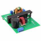
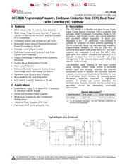
评估模块, 用于UCC28180功率因数校正控制器
Pictures:
3D模型
符号图
焊盘图
引脚图
产品图
页面导航:
引脚图在P3P4Hot
典型应用电路图在P1P21P22P23
原理图在P1P12P21
封装尺寸在P39P41P42
标记信息在P39
封装信息在P38P39P40P41P42
技术参数、封装参数在P4
应用领域在P1P45
电气规格在P5P6
导航目录
UCC28180EVM-573数据手册
Page:
of 45 Go
若手册格式错乱,请下载阅览PDF原文件
GND
ICOMP
ISENSE
GATE
VCC
VSENSE
VCOMP
FREQ
1
2
3
4
8
7
6
5
UCC28180
www.ti.com
SLUSBQ5B –NOVEMBER 2013–REVISED DECEMBER 2014
5 Description (Continued)
Simple external networks allow for flexible compensation of the current and voltage control loops. In addition,
UCC28180 offers an enhanced dynamic response circuit that is based on the voltage feedback signal to deliver
improved response under fast load transients, both for output overvoltage and undervoltage conditions. An
unique VCOMP discharge circuit provided in UCC28180 is activated whenever the voltage feedback signal
exceeds V
OVP_L
thus allowing a chance for the control loop to stabilize quickly and avoid encountering the
overvoltage protection function when PWM shutoff can often cause audible noise. Controlled soft start gradually
regulates the input current during start-up and reduces stress on the power switches. Numerous system-level
protection features available in the controller include VCC UVLO, peak current limit, soft overcurrent, output
open-loop detection, output overvoltage protection and open-pin detection (VISNS). A trimmed internal reference
provides accurate protection thresholds and regulation set-point. The user can control low-power standby mode
by pulling the VSENSE pin below 0.82 V.
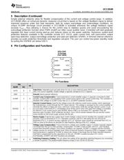
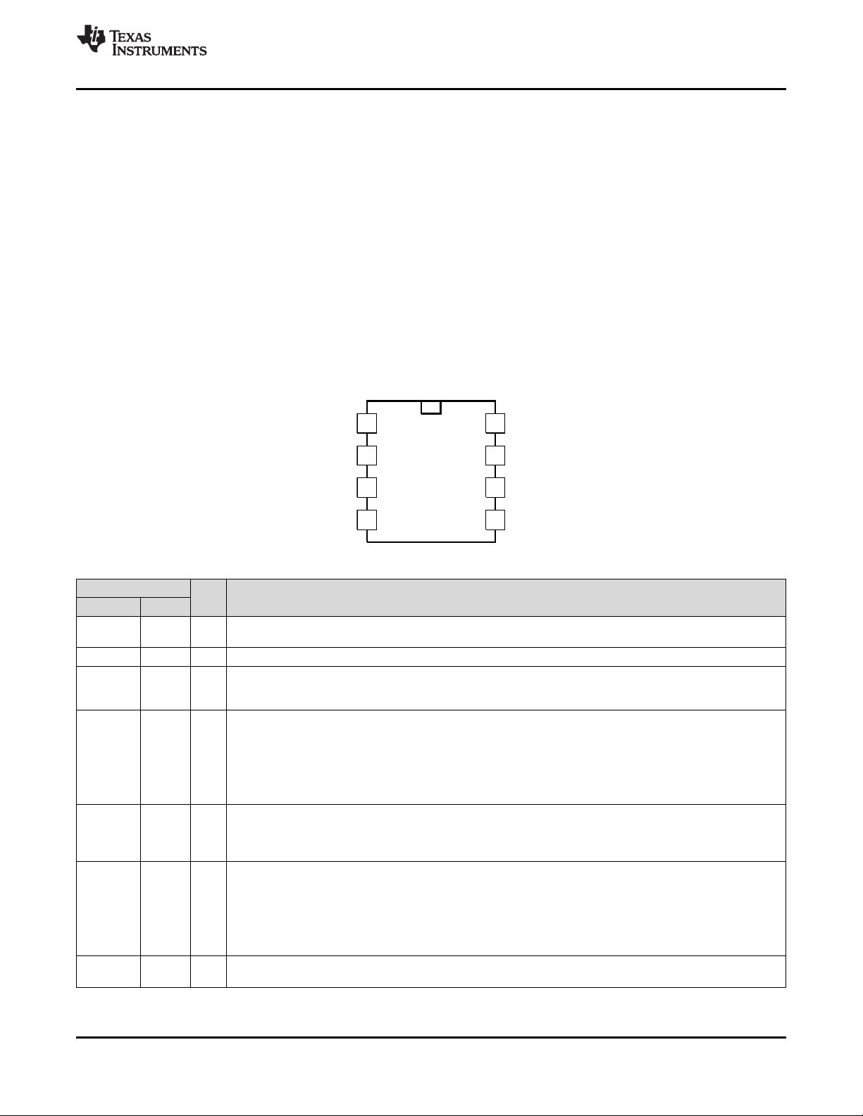
6 Pin Configuration and Functions
8-Pin SOIC
D Package
(TOP VIEW)
Pin Functions
PIN
I/O DESCRIPTION
NAME NO.
Gate Drive: Integrated push-pull gate driver for one or more external power MOSFETs. Typical 2.0-A sink
GATE 8 O
and 1.5-A source capability. Output voltage is typically clamped at 15.2 V (typical).
GND 1 Ground: device ground reference.
Current Loop Compensation: Transconductance current amplifier output. A capacitor connected to GND
ICOMP 2 O provides compensation and averaging of the current sense signal in the current control loop. The controller is
disabled if the voltage on ICOMP is less than 0.2 V, (ICOMPP protection function).
Inductor Current Sense: Input for the voltage across the external current sense resistor, which represents
the instantaneous current through the PFC boost inductor. This voltage is averaged by the current amplifier to
eliminate the effects of ripple and noise. Soft Over Current (SOC) limits the average inductor current. Cycle-
ISENSE 3 I by-cycle peak current limit (PCL) immediately shuts off the GATE drive if the peak-limit voltage is exceeded.
An internal 2.3-µA current source pulls ISENSE above 0.085 V to shut down PFC operation if this pin
becomes open-circuited, (ISOP protection function). Use a 220-Ω resistor between this pin and the current
sense resistor to limit inrush-surge currents into this pin.
Device Supply: External bias supply input. Under-Voltage Lockout (UVLO) disables the controller until VCC
exceeds a turn-on threshold of 11.5 V. Operation continues until VCC falls below the turn-off (UVLO)
VCC 7
threshold of 9.5 V. A ceramic by-pass capacitor of 0.1 µF minimum value should be connected from VCC to
GND as close to the device as possible for high-frequency filtering of the VCC voltage.
Voltage Loop Compensation: Transconductance voltage error amplifier output. A resistor-capacitor network
connected from this pin to GND provides compensation. VCOMP is held at GND until VCC, and VSENSE
exceed their threshold voltages. Once these conditions are satisfied, VCOMP is charged until the VSENSE
VCOMP 5 O voltage reaches its nominal regulation level. When Enhanced Dynamic Response (EDR) is engaged, a higher
transconductance is applied to VCOMP to reduce the charge or discharge time for faster transient response.
Soft Start is programmed by the capacitance on this pin. VCOMP is pulled low when VCC UVLO,
OLP/Standby, ICOMPP and ISOP functions are activated.
Switching Frequency Setting: This pin allows the setting of the operating switching frequency by connecting
FREQ 4 O
a resistor to ground. The programmable frequency range is from 18 kHz to 250 kHz.
Copyright © 2013–2014, Texas Instruments Incorporated Submit Documentation Feedback 3
Product Folder Links: UCC28180
器件 Datasheet 文档搜索
AiEMA 数据库涵盖高达 72,405,303 个元件的数据手册,每天更新 5,000 多个 PDF 文件
