Datasheet 搜索 > 开发板 > TI(德州仪器) > UCC28180EVM-573 数据手册 > UCC28180EVM-573 用户编程技术手册 4/45 页

¥ 37.945
UCC28180EVM-573 用户编程技术手册 - TI(德州仪器)
制造商:
TI(德州仪器)
分类:
开发板
描述:
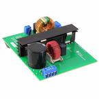
评估模块, 用于UCC28180功率因数校正控制器
Pictures:
3D模型
符号图
焊盘图
引脚图
产品图
页面导航:
引脚图在P3P4Hot
典型应用电路图在P1P21P22P23
原理图在P1P12P21
封装尺寸在P39P41P42
标记信息在P39
封装信息在P38P39P40P41P42
技术参数、封装参数在P4
应用领域在P1P45
电气规格在P5P6
导航目录
UCC28180EVM-573数据手册
Page:
of 45 Go
若手册格式错乱,请下载阅览PDF原文件

UCC28180
SLUSBQ5B –NOVEMBER 2013–REVISED DECEMBER 2014
www.ti.com
Pin Functions (continued)
PIN
I/O DESCRIPTION
NAME NO.
Output Voltage Sense: An external resistor-divider network connected from this pin to the PFC output
voltage provides feedback sensing for regulation to the internal 5-V reference voltage. A small capacitor from
this pin to GND filters high-frequency noise. Standby disables the controller and discharges VCOMP when
the voltage at VSENSE drops below the Open-Loop Protection (OLP) threshold of 16.5%V
REF
(0.82 V). An
internal 100-nA current source pulls VSENSE to GND during pin disconnection. Enhanced Dynamic
VSENSE 6 I
Response (EDR) rapidly returns the output voltage to its normal regulation level when a system line or load
step causes VSENSE to rise above 105% or fall below 95% of the reference voltage. Two level Output Over-
Voltage Protection (OVP): a 4-kΩ resistor connects VCOMP to ground to rapidly discharge VCOMP when
VSENSE exceeds 107% (V
OVP_L
) of the reference voltage. If VSENSE exceeds 109% (V
OVP_H
) of the
reference voltage, GATE output will be disabled until VSENSE drops below 102% of the reference voltage.
7 Specifications
7.1 Absolute Maximum Ratings
(1)
Over operating free-air temperature range, all voltages are with respect to GND (unless otherwise noted). Currents are
positive into and negative out of the specified terminal.
MIN MAX UNIT
Input voltage range VCC, GATE –0.3 22 V
FREQ, VSENSE, VCOMP, ICOMP –0.3 7
ISENSE –24 7
Input current range VSENSE, ISENSE –1 1 mA
Junction temperature, T
J
Operating –55 150 °C
Lead temperature, T
SOL
Soldering, 10 s 300 °C
Storage temperature, T
stg
–65 150 °C
(1) Stresses beyond those listed under “absolute maximum ratings” may cause permanent damage to the device. These are stress ratings
only and functional operation of the device at these or any other condition beyond those included under “recommended operating
conditions” is not implied. Exposure to absolute-maximum-rated conditions for extended periods of time may affect device reliability.
7.2 ESD Ratings
VALUE UNIT
Human-body model (HBM), per ANSI/ESDA/JEDEC JS-001
(1)
±2000
V
(ESD)
Electrostatic discharge V
Charged-device model (CDM), per JEDEC specification JESD22- ±500
C101
(2)
(1) JEDEC document JEP155 states that 500-V HBM allows safe manufacturing with a standard ESD control process.
(2) JEDEC document JEP157 states that 250-V CDM allows safe manufacturing with a standard ESD control process.
7.3 Recommended Operating Conditions
over operating free-air temperature range (unless otherwise noted)
MIN MAX UNIT
VCC input voltage from a low-impedance source VCC
OFF
+ 1V 21 V
Operating junction temperature, T
J
–40 125 °C
Operating frequency 18 250 kHz
4 Submit Documentation Feedback Copyright © 2013–2014, Texas Instruments Incorporated
Product Folder Links: UCC28180
器件 Datasheet 文档搜索
AiEMA 数据库涵盖高达 72,405,303 个元件的数据手册,每天更新 5,000 多个 PDF 文件
