Datasheet 搜索 > NXP(恩智浦) > LPC2131FBD64 数据手册 > LPC2131FBD64 数据手册 9/45 页

¥ 0
LPC2131FBD64 数据手册 - NXP(恩智浦)
制造商:
NXP(恩智浦)
封装:
LQFP
描述:
NXP LPC2131FBD64 微控制器, 32位, ARM7TDMI, 60 MHz, 32 KB, 8 KB, 64 引脚, LQFP
Pictures:
3D模型
符号图
焊盘图
引脚图
产品图
页面导航:
导航目录
LPC2131FBD64数据手册
Page:
of 45 Go
若手册格式错乱,请下载阅览PDF原文件

LPC2131_32_34_36_38 All information provided in this document is subject to legal disclaimers. © NXP B.V. 2011. All rights reserved.
Product data sheet Rev. 5.1 — 29 July 2011 9 of 45
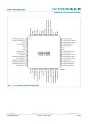
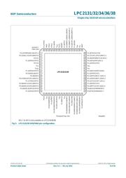
NXP Semiconductors
LPC2131/32/34/36/38
Single-chip 16/32-bit microcontrollers
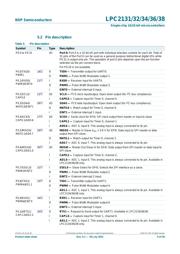
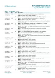
5.2 Pin description
Table 3. Pin description
Symbol Pin Type Description
P0.0 to P0.31 I/O Port 0: Port 0 is a 32-bit I/O port with individual direction controls for each bit. Total of
31 pins of the Port 0 can be used as a general purpose bidirectional digital I/Os while
P0.31 is output only pin. The operation of port 0 pins depends upon the pin function
selected via the pin connect block.
Pin P0.24 is not available.
P0.0/TXD0/
PWM1
19
[1]
O TXD0 — Transmitter output for UART0.
O PWM1 — Pulse Width Modulator output 1.
P0.1/RXD0/
PWM3/EINT0
21
[2]
I RXD0 — Receiver input for UART0.
O PWM3 — Pulse Width Modulator output 3.
I EINT0 — External interrupt 0 input.
P0.2/SCL0/
CAP0.0
22
[3]
I/O SCL0 — I
2
C0 clock input/output. Open drain output (for I
2
C-bus compliance).
I CAP0.0 — Capture input for Timer 0, channel 0.
P0.3/SDA0/
MAT0.0/EINT1
26
[3]
I/O SDA0 — I
2
C0 data input/output. Open drain output (for I
2
C-bus compliance).
O MAT0.0 — Match output for Timer 0, channel 0.
I EINT1 — External interrupt 1 input.
P0.4/SCK0/
CAP0.1/AD0.6
27
[4]
I/O SCK0 — Serial clock for SPI0. SPI clock output from master or input to slave.
I CAP0.1 — Capture input for Timer 0, channel 1.
I AD0.6 — ADC 0, input 6. This analog input is always connected to its pin.
P0.5/MISO0/
MAT0.1/AD0.7
29
[4]
I/O MISO0 — Master In Slave V
DD
= 3.6 V for SPI0. Data input to SPI master or data
output from SPI slave.
O MAT0.1 — Match output for Timer 0, channel 1.
I AD0.7 — ADC 0, input 7. This analog input is always connected to its pin.
P0.6/MOSI0/
CAP0.2/AD1.0
30
[4]
I/O MOSI0 — Master Out Slave In for SPI0. Data output from SPI master or data input to
SPI slave.
I CAP0.2 — Capture input for Timer 0, channel 2.
I AD1.0 — ADC 1, input 0. This analog input is always connected to its pin. Available in
LPC2134/36/38 only.
P0.7/SSEL0/
PWM2/EINT2
31
[2]
I SSEL0 — Slave Select for SPI0. Selects the SPI interface as a slave.
O PWM2 — Pulse Width Modulator output 2.
I EINT2 — External interrupt 2 input.
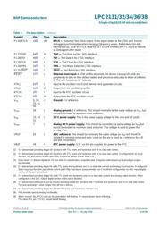
P0.8/TXD1/
PWM4/AD1.1
33
[4]
O TXD1 — Transmitter output for UART1.
O PWM4 — Pulse Width Modulator output 4.
I AD1.1 — ADC 1, input 1. This analog input is always connected to its pin. Available in
LPC2134/36/38 only.
P0.9/RXD1/
PWM6/EINT3
34
[2]
I RXD1 — Receiver input for UART1.
O PWM6 — Pulse Width Modulator output 6.
I EINT3 — External interrupt 3 input.
P0.10/RTS1/
CAP1.0/AD1.2
35
[4]
O RTS1 — Request to Send output for UART1. Available in LPC2134/36/38.
I CAP1.0 — Capture input for Timer 1, channel 0.
I AD1.2 — ADC 1, input 2. This analog input is always connected to its pin. Available in
LPC2134/36/38 only.
器件 Datasheet 文档搜索
AiEMA 数据库涵盖高达 72,405,303 个元件的数据手册,每天更新 5,000 多个 PDF 文件
