Datasheet 搜索 > 8位微控制器 > Microchip(微芯) > PIC16F1704T-I/ST 数据手册 > PIC16F1704T-I/ST 数据手册 11/472 页
 器件3D模型
¥ 8.323
PIC16F1704T-I/ST 数据手册 - Microchip(微芯)
制造商:
Microchip(微芯)
分类:
8位微控制器
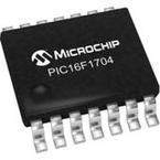
封装:
TSSOP-14
描述:
PIC 32MHz 闪存:4K@x14bit
Pictures:
3D模型
符号图
焊盘图
引脚图
产品图
页面导航:
引脚图在P3P11P12P13P14P15P16P147P170P272P274P369Hot
典型应用电路图在P157P370
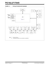
原理图在P10P17P55P64P76P99P139P148P154P160P162P169
封装尺寸在P442
标记信息在P439P440P441
封装信息在P439P443P444P446P447P449P452P453P454P455P469
技术参数、封装参数在P67P71P84P97P98P162P163P241P395P400P410P411
应用领域在P53
电气规格在P71P84P97P98
导航目录
PIC16F1704T-I/ST数据手册
Page:
of 472 Go
若手册格式错乱,请下载阅览PDF原文件
2013 Microchip Technology Inc. Preliminary DS40001715B-page 11
PIC16(L)F1704/8
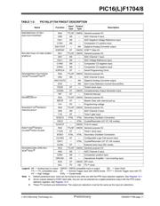
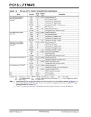
TABLE 1-2: PIC16(L)F1704 PINOUT DESCRIPTION
Name Function
Input
Type
Output
Type
Description
RA0/AN0/V
REF-/C1IN+/
DAC1OUT/ICSPDAT
RA0 TTL/ST CMOS General purpose I/O.
AN0 AN — ADC Channel 0 input.
V
REF- AN — ADC Negative Voltage Reference input.
C1IN+ AN — Comparator C1 positive input.
DAC1OUT — AN Digital-to-Analog Converter output.
ICSPDAT ST CMOS ICSP™ Data I/O.
RA1/AN1/V
REF+/C1IN0-/C2IN0-/
ICSPCLK
RA1 TTL/ST CMOS General purpose I/O.
AN1 AN — ADC Channel 1 input.
V
REF+ AN — ADC Voltage Reference input.
C1IN0- AN — Comparator C2 negative input.
C2IN0- AN — Comparator C3 negative input.
ICSPCLK ST — Serial Programming Clock.
RA2/AN2/DAC1OUT2/ZCD/
T0CKI
(1)
/COGIN
(1)
/INT
(1)
RA2 TTL/ST CMOS General purpose I/O.
AN2 AN — ADC Channel 2 input.
DAC1OUT2 — AN Digital-to-Analog Converter output.
ZCD — AN Zero Cross Detection Current Source/Sink.
T0CKI ST — Timer0 clock input.
COGIN ST CMOS Complementary Output Generator input.
INT ST — External interrupt.
RA3/MCLR
/VPP RA3 TTL/ST CMOS General purpose I/O.
MCLR
ST — Master Clear with internal pull-up.
V
PP HV — Programming voltage.
RA4/AN3/T1G
(1)
/SOSCO/
OSC2/CLKOUT
RA4 TTL/ST CMOS General purpose I/O.
AN3 AN — ADC Channel 3 input.
T1G ST — Timer1 gate input.
SOSCO XTAL XTAL Secondary Oscillator Connection.
OSC2 — XTAL Crystal/Resonator (LP, XT, HS modes).
CLKOUT — CMOS F
OSC/4 output.
RA5/T1CKI
(1)
/SOSCI/
CLCIN3
(1)
/OSC1/CLKIN
RA5 TTL/ST CMOS General purpose I/O.
T1CKI ST — Timer1 clock input.
SOSCI XTAL XTAL Secondary Oscillator Connection.
CLCIN3 ST — Configurable Logic Cell source input.
OSC1 — XTAL Crystal/Resonator (LP, XT, HS modes).
CLKIN ST — External clock input (EC mode).
RC0/AN4/C2IN+/OPA1IN+/
SCK
(1)
/SCL
(3)
RC0 TTL/ST CMOS General purpose I/O.
AN4 AN — ADC Channel 4 input.
C2IN+ AN — Comparator positive input.
OPA1IN+
AN —
Operational Amplifier 1 non-inverting input.
SCK ST CMOS SPI clock.
SCL I
2
CODI
2
C™ clock.
Legend: AN = Analog input or output CMOS= CMOS compatible input or output OD = Open Drain
TTL = TTL compatible input ST = Schmitt Trigger input with CMOS levels I
2
C™ = Schmitt Trigger input with I
2
C
HV = High Voltage XTAL = Crystal levels
Note 1: Default peripheral input. Input can be moved to any other pin with the PPS input selection registers. See Register 12-1.
2: All pin outputs default to PORT latch data. Any pin can be selected as a digital peripheral output with the PPS output
selection registers. See Register 12-3.
3: These I
2
C functions are bidirectional. The output pin selections must be the same as the input pin selections.
器件 Datasheet 文档搜索
AiEMA 数据库涵盖高达 72,405,303 个元件的数据手册,每天更新 5,000 多个 PDF 文件
