Datasheet 搜索 > 存储芯片 > Microchip(微芯) > 24AA01T-I/ST 数据手册 > 24AA01T-I/ST 其他数据使用手册 6/47 页
 器件3D模型
¥ 2.481
24AA01T-I/ST 其他数据使用手册 - Microchip(微芯)
制造商:
Microchip(微芯)
分类:
存储芯片
封装:
TSSOP-8
描述:
8 TSSOP 4.4mm 1K 128x8 卷盘
Pictures:
3D模型
符号图
焊盘图
引脚图
产品图
页面导航:
导航目录
24AA01T-I/ST数据手册
Page:
of 47 Go
若手册格式错乱,请下载阅览PDF原文件
2009-2021 Microchip Technology Inc. DS20001711M-page 6
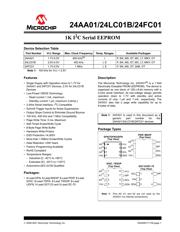
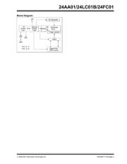
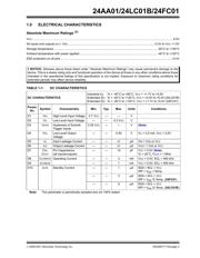
24AA01/24LC01B/24FC01
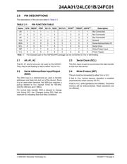
2.0 PIN DESCRIPTIONS
The descriptions of the pins are listed in Tab le 2- 1.
TABLE 2-1: PIN FUNCTION TABLE
2.1 A0, A1, A2
The A0, A1 and A2 pins are not used by the 24XX01.
They may be left floating or tied to either V
SS or VCC.
2.2 Serial Address/Data Input/Output
(SDA)
The SDA input is a bidirectional pin used to transfer
addresses and data into and out of the device. Since
it is an open-drain terminal, the SDA bus requires a
pull-up resistor to V
CC (typical 10 kΩ for 100 kHz,
2kΩ for 400 kHz and 1 MHz).
For normal data transfer, SDA is allowed to change
only during SCL low. Changes during SCL high are
reserved for indicating Start and Stop conditions.
2.3 Serial Clock (SCL)
The SCL input is used to synchronize the data transfer
to and from the device.
2.4 Write-Protect (WP)
This pin must be connected to either VSS or VCC.
If tied to V
SS, normal memory operation is enabled
(read/write the entire memory 00-7F).
If tied to V
CC, write operations are inhibited. The entire
memory will be write-protected. Read operations are
not affected.
Name DFN MSOP PDIP SC-70 SOIC SOT-23 TDFN
(1)
TSSOP UDFN
(1)
Description
A0 1 1 1 — 1 — 1 1 1 Not Connected
A1 2 2 2 — 2 — 2 2 2 Not Connected
A2 3 3 3 — 3 — 3 3 3 Not Connected
VSS 4 4 4 2 4 2 4 4 4 Ground
SDA 5 5 5 3 5 3 5 5 5 Serial Address/Data I/O
SCL 6 6 6 1 6 1 6 6 6 Serial Clock
WP 7 7 7 5 7 5 7 7 7 Write-Protect Input
V
CC 8 8 8 4 8 4 8 8 8 Power Supply
Note 1: The exposed pad on the TDFN/UDFN package can be connected to V
SS or left floating.
器件 Datasheet 文档搜索
AiEMA 数据库涵盖高达 72,405,303 个元件的数据手册,每天更新 5,000 多个 PDF 文件
