Datasheet 搜索 > 存储芯片 > Microchip(微芯) > 25LC128T-I/ST 数据手册 > 25LC128T-I/ST 其他数据使用手册 2/32 页
 器件3D模型
¥ 9.491
25LC128T-I/ST 其他数据使用手册 - Microchip(微芯)
制造商:
Microchip(微芯)
分类:
存储芯片
封装:
TSSOP-8
描述:
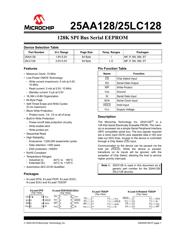
128 K SPI总线 串行EEPROM
Pictures:
3D模型
符号图
焊盘图
引脚图
产品图
页面导航:
导航目录
25LC128T-I/ST数据手册
Page:
of 32 Go
若手册格式错乱,请下载阅览PDF原文件
2003-2019 Microchip Technology Inc. DS20001831F-page 2
25AA128/25LC128
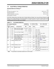
1.0 ELECTRICAL CHARACTERISTICS
Absolute Maximum Ratings
(†)
VCC.............................................................................................................................................................................6.5V
All inputs and outputs w.r.t. V
SS ..........................................................................................................-0.6V to VCC +1.0V
Storage temperature ................................................................................................................................. -65°C to 150°C
Ambient temperature under bias............................................................................................................... -40°C to 125°C
ESD protection on all pins.......................................................................................................................................... 4 kV
† NOTICE: Stresses above those listed under “Absolute Maximum Ratings” may cause permanent damage to the
device. This is a stress rating only and functional operation of the device at those or any other conditions above those
indicated in the operational listings of this specification is not implied. Exposure to maximum rating conditions for an
extended period of time may affect device reliability.
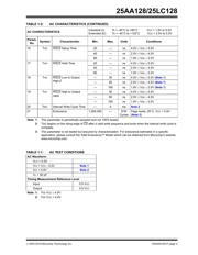
TABLE 1-1: DC CHARACTERISTICS
DC CHARACTERISTICS
Industrial (I): T
A = -40°C to +85°C VCC = 1.8V to 5.5V
Extended (E): T
A = -40°C to +125°C VCC = 2.5V to 5.5V
Param.
No.
Symbol Characteristic Min. Max. Units Conditions
D1 V
IH High-Level Input Voltage 0.7 VCC VCC+1 V
D2 VIL1 Low-Level Input Voltage -0.3 0.3 VCC VVCC2.7V
D3 V
IL2 -0.3 0.2 VCC VVCC < 2.7V
D4 VOL Low-Level Output Voltage — 0.4 V IOL = 2.1 mA
D5 VOL —0.2VIOL = 1.0 mA, VCC < 2.5V
D6 V
OH High-Level Output Voltage VCC -0.5 — V IOH = -400 µA
D7 ILI Input Leakage Current — ±1 µA CS = VCC, VIN = VSS or VCC
D8 ILO Output Leakage Current — ±1 µA CS = VCC, VOUT = VSS or VCC
D9 CINT Internal Capacitance
(all inputs and outputs)
—7pFTA = 25°C, CLK = 1.0 MHz,
V
CC = 5.0V (Note)
D10 ICC Read Operating Current — 5 mA VCC = 5.5V, FCLK = 10.0 MHz,
SO = Open
—2.5mAV
CC = 2.5V, FCLK = 5.0 MHz
SO = Open
D11 I
CC Write Operating Current — 5 mA VCC = 5.5V
—3mAVCC = 2.5V
D12 I
CCS Standby Current — 5 µA CS = VCC = 5.5V, Inputs tied to VCC
or V
SS, 125°C
—1µACS = VCC = 5.5V, Inputs tied to VCC
or V
SS, 85°C
Note: This parameter is periodically sampled and not 100% tested.
器件 Datasheet 文档搜索
AiEMA 数据库涵盖高达 72,405,303 个元件的数据手册,每天更新 5,000 多个 PDF 文件
